Research
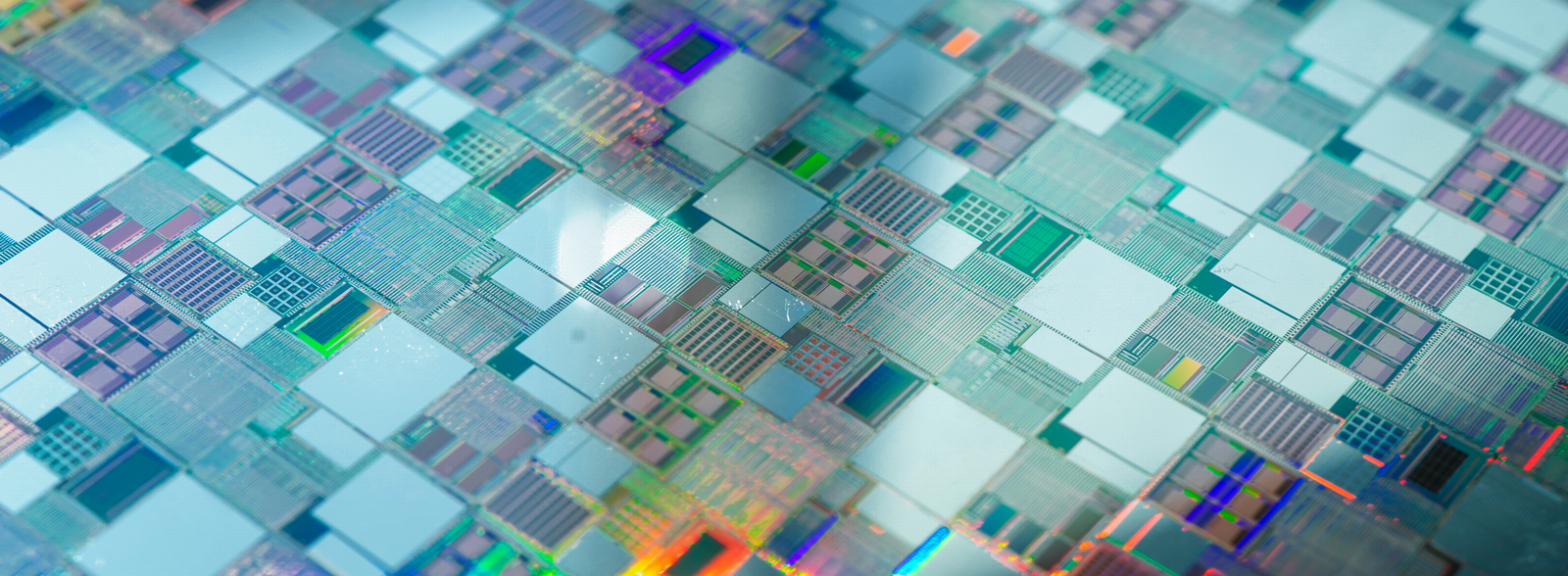
Semiconductors have been around for less than a century, yet they have already become an indispensable part of our daily lives. This is because semiconductor technology is highly versatile, governing information, light, and energy. While silicon (Si) has traditionally been the primary material and is expected to remain so, MOS transistors —the building blocks of logic circuits in smartphones and PCs— have evolved from conventional planar structures to FinFETs, and now to three-dimensional structures with stacked nanosheets (GAA: Gate-All-Around). Thinner nanosheets help suppress short-channel effects; however, when the thickness of a Si sheet falls below 4 nm, the carrier mobility severely degrades due to microscopic variations in thickness. Therefore, nanosheets with a thickness of 3 nm or less that maintain high carrier mobility are highly demanded. Atomically flat two-dimensional (2D) materials, such as transition metal dichalcogenides (TMDs) like MoS2 and WSe2, hold great promise. Developing alternative nanosheet materials to replace Si and establishing their device fabrication processes represent critical challenges.
In addition, in the field of power electronics for power conversion and control, innovations driven by wide-bandgap semiconductors like silicon carbide (SiC) and gallium nitride (GaN) are underway. Furthermore, next-generation materials such as gallium oxide and diamond are attracting significant attention. Leveraging the process technologies and device physics cultivated in silicon semiconductors, our group aims to create innovative devices that exploit the physical properties of these novel materials. We are currently focusing on the following three research themes.
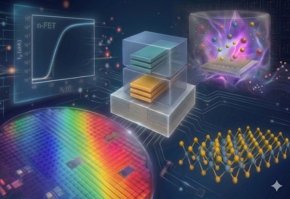
CFET Fabrication with New Material Integration
Complementary FET (CFET) technology, which vertically stacks p-channel and n-channel transistors instead of arranging them horizontally,
dramatically increases integration density. Active research and development are underway worldwide for its mass production in the early 2030s.
However, considering that channel materials are likely to transition to 2D materials from the mid-to-late 2030s—shortly
after the initial commercialization of CFETs—it is already necessary to develop CFET fabrication technologies geared toward this new material integration.
Our group participates in the
JST-Research and Development Program for Next-generation Edge AI Semiconductors and is actively working to establish the
"Fabrication Platform for Novel Material CFETs" at NIMS.
Germanium Nanosheets and Germanene
The world's first transistor demonstrated in 1947 utilized germanium (Ge) (leading to the 1956 Nobel Prize in Physics).
Ge belongs to Group IV, alongside carbon (C) and silicon (Si). It is an excellent semiconductor material with higher electron and hole mobilities than Si.
However, due to its sensitivity to fabrication processes and the difficulty in controlling its characteristics, Ge eventually yielded its dominant position
to Si. In recent years, as the thinning of Si nanosheets approaches its physical limit as mentioned above, Ge has garnered renewed attention through
the thinning of Ge nanosheets. Ge exhibits significantly higher mobility than Si, and a 2 nm-thick Ge(111) nanosheet is theoretically predicted to have
ten times the mobility of a Si nanosheet. However, fabricating Ge nanosheets is extremely difficult, and such predicted high mobilities have not yet been
experimentally confirmed. This difficulty stems from crystal damage during the thinning of single-crystal Ge and the challenges in achieving flat growth
due to Stranski-Krastanov (S-K) growth, which involves island formation.
Meanwhile, graphene, which won the Nobel Prize in Physics in 2010, is a 2D material consisting of carbon atoms arranged in a honeycomb lattice.
"Germanene," which replicates this honeycomb structure using Ge atoms, has also been experimentally verified.
However, it can currently only be synthesized on metal substrates and oxidizes easily, leaving its electronic properties largely uncharacterized.
Our group is tackling the challenge of developing "novel formation methodologies" for both Ge nanosheets and germanene.
Critical Challenges in SiC power MOSFET:SiO2/SiC interface
Silicon carbide (SiC) power devices are becoming increasingly ubiquitous, seeing adoption in railway vehicles and electric vehicles (EVs).
While SiC MOS transistors serve as core components of inverters—the key to low power consumption—their SiO2/SiC interface properties
along the on-state current path remain inadequate. Consequently, they cannot fully deliver their intrinsic performance, leaving substantial room for improvement.
To improve the SiO2/SiC interface properties, our group comprehensively conducts research on establishing new processes
(including novel oxidation methods), physical analysis of interface structures, device prototyping, and evaluation of electrical characteristics and reliability.