Research
1. Neuromorphic devices using spatiotemporal dynamics of ions and electrons
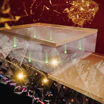
Recently, the problems of high power consumption, high transmission and high latency in machine learning have become increasingly serious. To solve this problem, we are developing neuromorphic devices that use the spatiotemporal dynamics of ions and electrons at ion-conductor interfaces and surfaces to perform information processing as efficiently as the human brain. We aim to create high-performance, highly integrated AI devices that can be used in a wide range of applications using an electric double layer only a few nanometres thick and a few organic molecules as computational resources.
Publications: Sci. Adv. (2024),Sci. Adv. (2022),Sci. Adv. (2018)
2. Ultrafast physical computing devices using spin-wave interference.
Interference of fast, fine spin waves (magnon) occurring within a magnetic body, like a water pattern, produces complex and diverse (chaotic) output responses. We have applied this mechanism to brain-type information processing and found that highly accurate time-series pattern prediction is possible. Research is underway to develop ultrafast physical computing devices with low power consumption and operating at high frequencies above GHz.
Publications: Adv. Sci. (2025), Mater. Today. Phys. (2024), Adv. Intell. Syst. (2023)
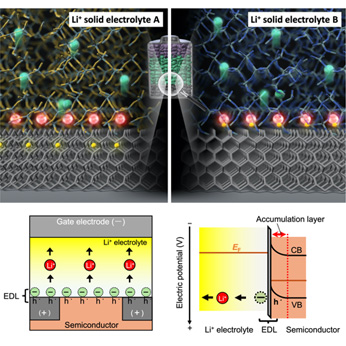
3. Analysis of the electric double layer・space charge layer at the solid electrolyte interface
All-solid-state batteries are the most promising candidate for next-generation batteries and are expected to find a wide range of applications, including electric vehicles. One of the issues is the power output reduction due to the high interface resistance at the solid electrolyte/electrode interface, which is suspected to be partly caused by the electric double layer・space charge layer due to the change in ion concentration near the interface, but the details are not yet known. We are analyzing the space charge layer at the solid electrolyte interface by applying the mechanism of field-effect transistors, which is a technique of semiconductor technology, to contribute to the higher power output of all-solid-state batteries.
Publications: Commun. Chem.(2021),
Mater. Today Phys. (2023), Mater. Today Adv. (2023)
4. Physical properties tuning devices using electric double layer effect and Redox reaction
At the ionic conductor/electronic material interface, high-density electron carriers exceeding 1021 cm-3 can be doped into the electronic material through the electric double-layer effect caused by the accumulation and depletion of mobile ions in the ionic conductor at the interface and redox reactions due to ion insertion and desertion into the electronic material, resulting in new electronic properties that cannot be obtained in bulk materials, or to a drastic change in electronic properties. We are investigating physical properties tuning devices that utilize the interfacial functionality of such ionic conductors.
Publications: Nano Lett. (2024), ACS Nano (2020)
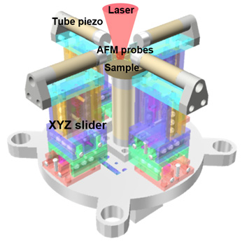
5. Direct measurement of electrical properties of nanomaterials with multiple-probe AFM
The electrical properties of novel nanomaterials need to be characterized, but electrode mounting may be difficult with conventional lithography techniques for some nanomaterials. To investigate the electrical properties of such nanomaterials, we have developed a multiple-probe AFM with four probes that can be driven independently, enabling direct electrical measurement with nanoscale positional accuracy. For example, it is possible to perform a four-probe measurement of a single-walled carbon nanotube with a diameter of approximately 1 nm. Furthermore, Raman spectroscopy of nanomaterials during electrical measurements is possible, providing information on their structure and composition.
Publications: Jpn. J. Appl. Phys. (2016), Adv. Mater. (2012)
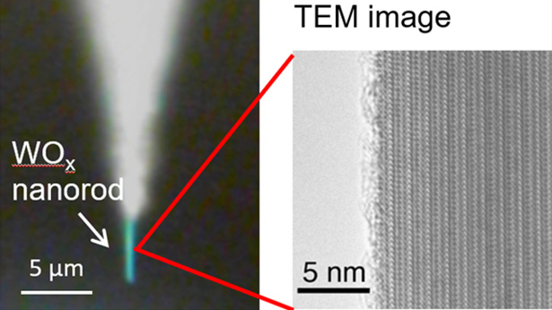
6. Single-molecule sensing using Raman scattering enhancement of WOx nanorods
There are many systems in which extremely small amounts of molecules play important roles, such as living cells, catalyst surfaces, and electrode surfaces. We have developed a sensor technology that enables us to understand the spatio-temporal behavior of various molecules in such systems. WOx nanorods with two-dimensional conducting planes in the crystal have large enhancement effect of Raman scattering due to plasmon resonance, which enables identification and detection of single molecules. Furthermore, by attaching the WOx nanorods to the tip of an AFM probe, we expect to realize high-spatial-resolution sensing.
Publications: Nanoscale (2022)
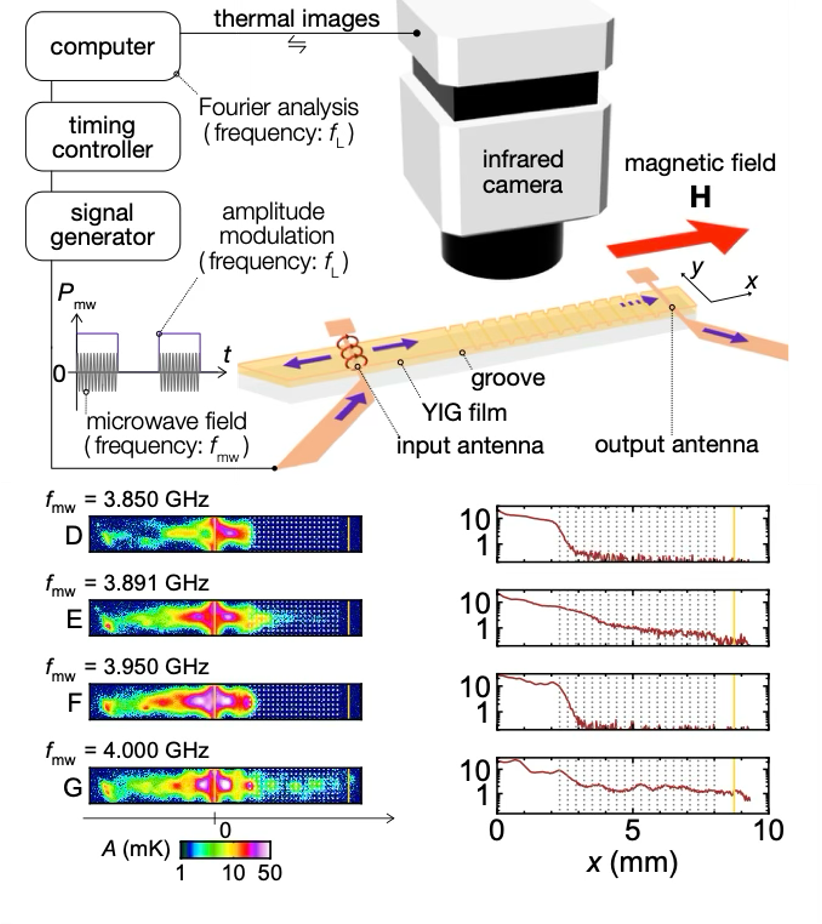
7. Dynamics of Magnetic and Dielectric Materials Observed Through Heat
In magnetic and dielectric materials, the degrees of freedom of magnetization and polarization respectively enable various functions through their motions. When magnetization or polarization moves, heat is generated as a result. For example, after the propagation of spin waves, heat arises like footprints through the spin relaxation process. In an example using thermography, periodic heat patterns caused by spin wave interference can be measured. By elucidating the dynamics through spatiotemporal thermal measurements, we aim to contribute to device development and pioneer new information carriers.
Publications: Phys. Rev. B (2020), Appl. Phys. Lett (2021), J. Appl. Phys. (2022)