Nano Electronics Device Materials Group
STAFF
NAGATA, Takahiro; KINO, Hiori; YAGYU, Shinjiro; YAMASHITA, Yoshiyuki(Staff Tabs)
AIM and GOAL
Nanoelectronics materials have been applied to various new devices for IoT, electric vehicle and so on. For these applications, demands of high reliability, high-speed operation, and high power are increasing. Our group focuses on thin-film dielectric materials in electronic materials with the aim of developing new thin-film materials that contribute to high reliability and next-generation high-speed/high-power electronic devices. Using combinatorial material development and interface evaluation techniques, we develop electronic materials that contribute to next-generation semiconductor devices such as film capacitors, memory devices, and high-k materials.

FIG1 Our research targets
APPROACH
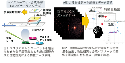
To accelerate the development of thin film materials, we are combining our combinatorial materials synthesis/evaluation technology with materials informatics. In addition, in the device application of new materials, the interfacial properties affect the physical and electrical properties. We have elucidated the electronic and defect structures of various interfaces using in-situ observation techniques, in particular the application of voltage using photoelectron spectroscopy. We will verify and solve problems in the development of new materials and device applications through the collaboration of synthesis, evaluation, and data science.

FIG2 Schematic of data-driven materials development combining combinatorial methods (upper) and optimization of dopants to re
Page top /Organization / Staff / Materials / Methods
NAGATA, Takahiro:Group Leader
Email: NAGATA.Takahiro@nims.go.jp

Page top /Organization / Staff / Materials / Methods

YAGYU, Shinjiro
Email: YAGYU.Shinjiro@nims.go.jp


Page top /Organization / Staff / Materials / Methods
YAMASHITA, Yoshiyuki
Email: YAMASHITA.Yoshiyuki@nims.go.jp


Page top /Organization / Staff / Materials / Methods