About our Lab.
Top> About our Lab.
Research outline
Semiconductor nanostructures are of great interest due to their novel physical properties and potential applications in electronic, optical, thermoelectric and bio.chemical sensing devices. We develop new functional nanostructures by constructing composite nanostructures. We have two main goals: 1) nano-electronics which based on semiconductor transistors, and 2) energy harvesting and storage solar cells. We are paving the way for these fields and constantly expanding to new subjects of research.
Research Goals
Development of the next-generation semiconductor materials
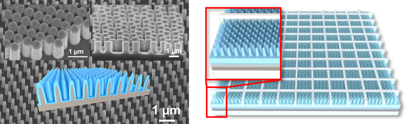
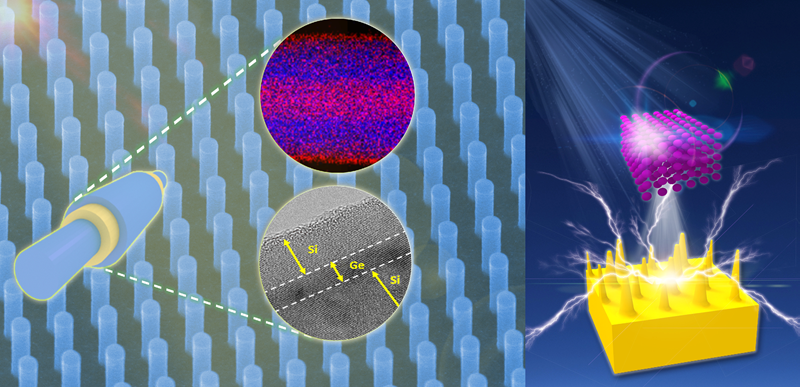
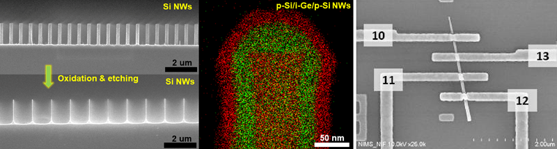
Improvements in performance and integration in planar MOSFETs by conventional scaling of device geometries are now reaching the practical limits. Core-shell nanowires are a key structure in realizing high mobility transistor channels since site-selective doping and band-offset in core-shell nanowires can divide the carrier transport region from the impurity doped region, resulting in the suppression of impurity scattering. Now we are constructing new transistor channels base on core-shell nanowires.
Furthermore, we are also interested in GeSn, a new group-IV semiconductor material, which opens up the possibility for optical devices and high-speed electronics.
Development of next-generation energy-related materials
Nanostructured materials have the potential to improve performance and introduce new functionality to energy-related devices. We are currently developing the next-generation photovoltaic cells using functionalized semiconductor nanostructures to realize both low-cost and high efficiency. In addition to energy harvesting, we are also interested in energy storage such as batteries. We are developing new Si-related nanocomposite materials with higher capacity and longer cycle properties.