Project Summary


Combinatorial material synthesis and application to the high performance electronics devices
Development of functional three-dimensional nanostructure fabrication technique for future devices
Molecular arrangement for device development
Development of organic molecular functional devices
Well-controlled growth of epitaxial ultrathin alumina films
Nanoscale measurement and control of work function and manipulation of molecular adsorption sites
Combinatorial material synthesis and application to the high performance electronics devices
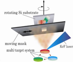
Combinatorial technique
Automated masks, substrate rotation and revolving targets make high throughput material synthesis possible.
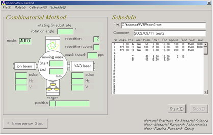
"Combinatorial Ware"
Depositions are carried out automatically using this software.
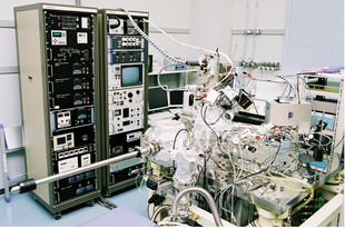
PLD Combinatorial Deposition System for Oxides
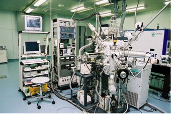
Dual Beam Combinatorial Deposition System
This system has both PLD and sputtering sources.
Excimer laser for PLD
Hi-performance XRD system
Development of functional three-dimensional nanostructure fabrication technique for future devices
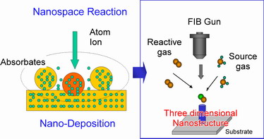
FIB method
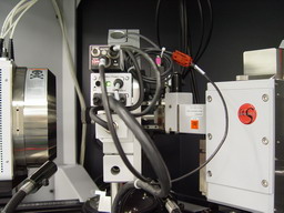
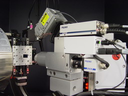
FIB-CVD System
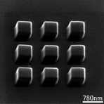
GaN-based three-dimensional nanostructure
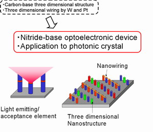
Development of high functional three-dimensional nanostructures
Combinatorial material synthesis and application to the high performance electronics devices
Development of functional three-dimensional nanostructure fabrication technique for future devices
Molecular arrangement for device development
Development of organic molecular functional devices
Well-controlled growth of epitaxial ultrathin alumina films
Nanoscale measurement and control of work function and manipulation of molecular adsorption sites
Molecular arrangement for device development
Precise control of molecular arrangement is required to make the most of molecular function and to develop molecular devices. In order to control the arrangement, including single-molecular distribution, one-dimensional wiring and two-dimensional array formation, intermolecular interaction and molecule-substrate interaction should be optimized. For this purpose, the structure of molecules are designed and synthesized. An UHV- STM is utilized to examine the molecular arrangement on metal, semiconductor and insulator substrates.
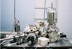
UHV-STM System
Substrate preparation, molecular deposition and STM observation can be carried out in ultrahigh vacuum.
Analysis and Control of Molecular arrangement
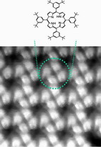
STM image of a porphyrin derivative on Cu(100) substrate and its structure.
Highly symmetric molecular structure resulted in well-ordered array formation on substrate.

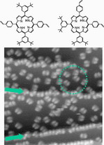
STM image of porphyrin derivatives with lower symmetric structure.
Each molecule distributes in a single-molecule on the terraces(Circle), whereas one-dimensional chains are formed along the step edges(Arrows).

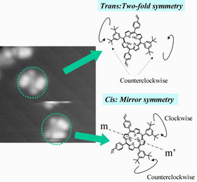
Structural characterization of individual molecules by high-resolution imaging.
Isomers of the derivatives show different symmetry, according to the rotational direction of the substituents.
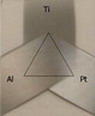
Development of Highly Functional Devices with C60
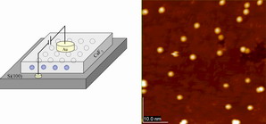
Monodispersed C60 molecules on CaF2/Si(111) substrate.
C60 molecules monodispersed in insulator layer act as Coulomb islands.
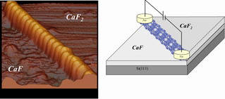
C60 "Chain" on CaF2/Si(111) substrate.
One-dimensional arrangement of C60 on insulator substrate has potential toward "Molecular Wiring".
Development of organic molecular functional devices
An advantage of organic materials is opto-electronic functions can be involved in each individual molecule. Meanwhile, such functions can also arise from highly-ordered assembly. We are investigating molecular devices, of which functions originating from individual molecules or from highly crystalline (highly pi-conjugated) assembly.
Combinatorial technique is applied for high throughput device development.
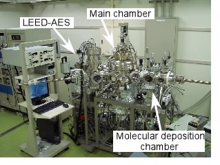
UHV-Organic MBE with LEED/AES.
Substrate preparation, molecular deposition and characterization can be carried out in ultrahigh vacuum.
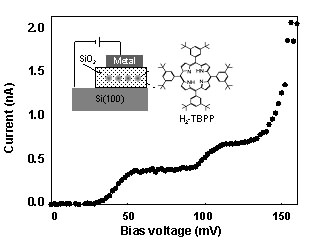
Single-electron device, where organic molecules act as Coulomb islands.
The device was fabricated by depositing insulator layers, molecules and metal films on Si(100) substrates.
Development to optical functional single-electron devices
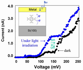
Light-induced change in tunneling process.
Light irradiation caused a reversible change in Coulomb blockade, demonstrating a potential of optical controllability of single-electron tunneling.
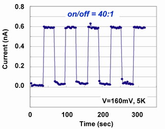
Optical switching of single-electron tunneling.
Electron-tunneling through molecular Coulomb island was controlled by light irradiation.
Combinatorial material synthesis and application to the high performance electronics devices
Development of functional three-dimensional nanostructure fabrication technique for future devices
Molecular arrangement for device development
Development of organic molecular functional devices
Well-controlled growth of epitaxial ultrathin alumina films
Nanoscale measurement and control of work function and manipulation of molecular adsorption sites
Well-controlled growth of epitaxial ultrathin alumina films
- toward the development of a tunneling electron emitter -
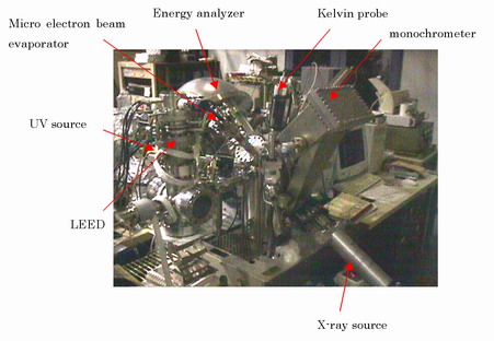
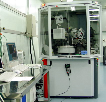
LEED/XPS/UPS/KP Combined system
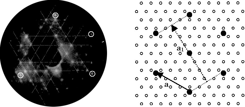
LEED pattern of alumina epitaxial thin film grown on CuAl alloy substrate
Nanoscale measurement and control of work function and manipulation of molecular adsorption sites
- Adsorption and reaction at nanostructured surface -
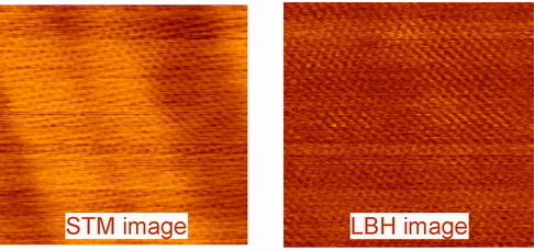
STM and LBH images of reconstructed Au(111) surface
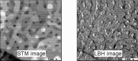
STM and LBH images of Au surface with nanopits
Combinatorial material synthesis and application to the high performance electronics devices
Development of functional three-dimensional nanostructure fabrication technique for future devices
Molecular arrangement for device development
Development of organic molecular functional devices
Well-controlled growth of epitaxial ultrathin alumina films
nanoscale measurement and control of work function and manipulation of molecular adsorption sites
Top of this page