MANA International Symposium 2025
Semiconductor Materials - 05
Title
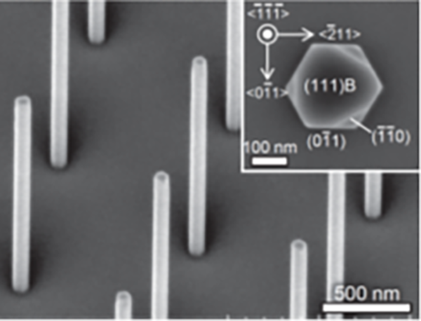
Selective-Area Growth of Semiconducting Nanowires

Authors
Affiliations
Semiconductor Nano-integration Group, MANA, NIMS
URL
https://www.nims.go.jp/group/Nano-integration/index-en.html
HARA.Shinjiro@nims.go.jp
Abstract
Semiconducting nanowires (NWs) have attracted great attention as a building block to improve the device performance associated with the miniaturization of transistors
Reference
- J. Svensson et al., Nano Lett. 15, 7898–7904 (2015). DOI: 10.1021/acs.nanolett.5b02936
- K. Ikejiri et al., J. Cryst. Growth 298, 616-619 (2007). DOI: 10.1016/j.jcrysgro.2006.10.179
- J. Noborisaka et al., Appl. Phys. Lett. 87, 093109 (2005). DOI: 10.1063/1.2035332
- K. Tomioka et al., Nano Lett. 8, 3475-3480 (2008). DOI: 10.1021/nl802398j
- S. Hara et al., (Invited Paper) J. Mater. Res. 34, 3863-3876 (2019). DOI: 10.1557/jmr.2019.333