MANA International Symposium 2025
Quantum Materials - 05
Title
Tunable carrier distribution 2D material device preparation by MOCVD
Authors
Affiliations
2D Quantum Materials Group, Quantum Materials Field, MANA
Nanoscience, Materials Chemistry and Engineering Course, Graduate School of Chemical Sciences and Engineering, Hokkaido University
URL
https://www.nims.go.jp/group/lowDmaterials/index-e.html
ZENG.Fanyu@nims.go.jp
Abstract
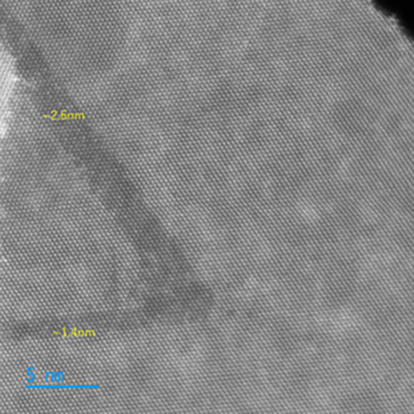
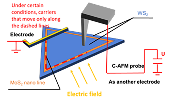
Carrier density is a crucial metric for semiconductor performance, often influencing device performance, reflecting the material‘s controllability and determining band filling and Fermi level, thereby influencing the material’s optical and electrical behavior. Two-dimensional materials are only one or a few atomic layers thick, so an external electric field can directly penetrate the entire material. The electric field has a significant impact on the distribution of electrons inside the material. Compared with three-dimensional materials, two-dimensional materials are more sensitive to changes in external electric fields. Therefore, applying an electric field to two-dimensional materials is an effective way to study carrier. Among many two-dimensional materials, TMDs (Transition Metal Dichalcogenides), with their two-dimensional structure and tunable properties, provide a unique platform for precisely controlling carrier behavior, making them key materials for next-generation electronic and optoelectronic devices. By using our laboratory’s advanced two-dimensional material MOCVD growth system, we have fabricated a single-layer two-dimensional heterostructure that WS2 with a nanoscale MoS2 channel embedded within it
Reference
- FANG.ZHANG, CRYSTAL GROWTH & DESIGN vol. 24 issue. 14, 6001-6006 (2024). DOI: 10.1021/acs.cgd.4c00477