Joint Workshop LANL/NIMS Quantum and Functional Materials and MANA International Symposium 2024
Session 3-3
Title
Ion Beam Synthesis of Layer-Tunable and Transfer Free Graphene for Device Applications
Authors
Yongqiang Wang
Affiliations
Los Alamos National Laboratory, Los Alamos, NM, USA
URL
https://cint.lanl.gov/facilities/general-ion-beam-mat-lab.shtml
yqwang@lanl.gov
Abstract
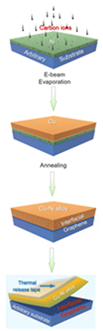
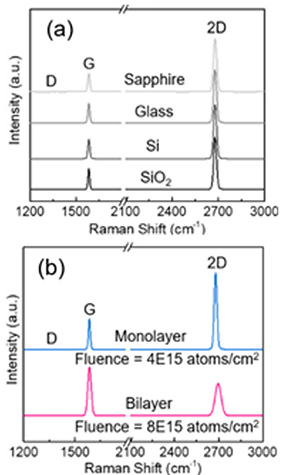
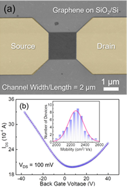
Direct synthesis of layer-tunable and transfer-free graphene on technologically important substrates is highly valued for various electronics and device applications. However, device relevant semiconductor/dielectric substrates pose challenges for chemical vapor deposition (CVD) since these types of materials are typically incapable of catalyzing the decomposition of carbon source gases and facilitating the adsorption and arrangement of active carbon atoms during CVD growth. State of the art in the field currently is a two-step process: a high-quality graphene layer synthesis on metal substrate through CVD followed by delicate layer-transfer onto device-relevant substrates.
Here we report a novel synthesis approach combining ion implantation for a precise graphene layer control and dual-metal smart Janus substrate for a diffusion-limiting graphene formation, to directly synthesize large area, high quality, and layer-tunable graphene films on device relevant substrates without the post-synthesis layer transfer process
Reference
- B.K. Wang, et al., Energy and Environmental Materials 7, e12730(2024). DOI: 10.1002/eem2.12730
- The abstract is approved for release by Los Alamos National Laboratory with LA-UR-24-28764.