Joint Workshop LANL/NIMS Quantum and Functional Materials and MANA International Symposium 2024


Session 1-2

Title

Low-temperature scanning tunneling microscopy of quantum materials

Author's photo

Authors

Shunsuke Yoshizawa

Affiliations

Center for Basic Research on Materials, NIMS

URL

https://samurai.nims.go.jp/profiles/yoshizawa_shunsuke

Email

YOSHIZAWA.Shunsuke@nims.go.jp

Abstract

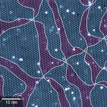
The scanning tunneling microscope (STM) allows us to probe electronic states near the Fermi energy with atomic-scale spatial resolution and plays an important role in the study of quantum materials. Our cryogenic, high-field STM system features low temperatures down to 0.4 K, high magnetic fields up to 16 T, and ultra-high vacuum chambers to prepare clean surfaces suitable for STM. The machine is currently being used to study various superconductors, topological insulators, atomic layer materials, etc., and here we would like to present some of our recent results.
One of them is on the transition metal dichalcogenide 2H-NbSe2, a layered compound that exhibits charge density waves (CDWs) below ~30 K. It also undergoes a superconducting transition at ~7 K and the superconductivity coexists with the CDW state. The interplay between the two coexisting states is attracting attention, and addressing this issue requires a detailed understanding of the CDW structure. Previous STM studies reported the existence of two types of lattice-commensurate CDW structures on the same surface, but the spatial distribution of their domains was not clearly resolved. We have obtained high-resolution STM images at 4.5 K and developed a numerical method to accurately determine the local CDW structure from the experimental image. We have unambiguously determined the spatial distribution of the domains and demonstrated the formation of alternating triangular domains of the two types of structures, as shown in Fig. 1 [1]. The structure is found to be consistent with the predictions of a phenomenological theory proposed before STM became widely used [2].

Fig. 1. STM image of 2H-NbSe2 recorded at 4.5 K, resolving the characteristic CDWs. The two types of domains are plotted in different colors.

Reference

  1. S, Yoshizawa, et al., Phy. Rev. Lett. 132, 056401 (2024). DOI: 10.1103/physrevlett.132.056401
  2. K. Nakanishi and H. Shiba, J. Phys. Soc. Jpn. 52, 1278 (1983). DOI: 10.1143/JPSJ.52.1278