Joint Workshop LANL/NIMS Quantum and Functional Materials and MANA International Symposium 2024


Quantum Materials - 20

Title

Resistance Switching in [6,6]-Phenyl C71 Butyric Acid Methyl Ester Thin Film

Author's photo

Authors

Kazuki Aihara1,2, Hiroshi Suga1,2, Kazuhito Tsukagoshi2,1

Affiliations

Chiba Institute of Technology1, MANA, NIMS2

URL


Email

TSUKAGOSHI.Kazuhito@nims.go.jp

Abstract

A fullerene nano-chain connected with metallic junction on silicon substrates has been realized using a derivative of fullerene with a carboxy group “Pyrrolidine Tris Acid (CPTA)” [1,2]. This fullerene nano-chain showed a resistance switch at room temperature. The resistance switch in nano-chain junction is not limited to C60 but should also occur in C70 fullerenes. In this research, we focused on the high electron-accepting ability of 70 and fabricated a fullerene resistive element using a C70 derivative, [6,6]-Phenyl C71 butyric acid methyl ester (PC71BM) and evaluated its switching behavior.
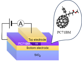
Figure 1 shows a schematic of the PC71BM device. Conductivity measurements were performed at room temperature in a vacuum environment (<1.0×10⁻² Pa), and when the voltage was applied to the devices, resistance switching was observed in the PC71BM devices as in the CPTA devices. Two resistance states of “High Resistance State (HRS)” and “Low Resistance State (LRS)” are switched by the application of voltage. Figure 2 (a) shows a typical I–V characteristic as set process, where the current shows transitions from LRS to LRS when voltage is applied. On the other hand, Fig. 2 (b) shows a typical I–V characteristic as reset process, where an increase in the applied voltage causes a sudden decrease, which is recognized as negative differential resistance (NDR) change from LRS to HRS. From distribution plots of turn-on and NDR peak voltages (Figs. 2(c) and 2(d)), average voltages of 2.9 V for turn-on voltage and 3.3 V for NDR peak were obtained. The switching voltages of these C70-based PC71BMs tend to operate at lower voltages than those of the C60-based CPTAs investigated so far.

Fig. 1. Schematic of PC71BM switching device. A PC71BM film was used for switching channel. The channel area in the PC71BM film was electrically activated by electron beam irradiation.
Fig. 2. I-V characteristic of PC71BM switching operation. (a) Transition to Low Resistance. (b) Transition to High Resistance. (c) Histogram of Turn-on Voltage. (d) Histogram of NDR peak Voltage.

Reference

  1. M. Takei, H. Suga, K.Tsukagoshi, et al., ACS Appl. Electron. Mater. 6, 1740, (2024). DOI 10.1021/acsaelm.3c01656
  2. T. Hirama, H. Suga, K.Tsukagoshi, et al., ACS Appl. Electron. Mater. 6, 3404, (2024). DOI 10.1021/acsaelm.4c00219