Joint Workshop LANL/NIMS Quantum and Functional Materials and MANA International Symposium 2024


Quantum Materials - 18

Title

Carbonized Peptide Microspheres: Advanced Metal-Free Fluorescent Micro-Emitters for Encrypted Photonic Barcodes and Anti-Counterfeit Solutions

Author's photo

Authors

Barun Kumar Barmana*, Keisuke Watanabea, Tadaaki Nagaoa,b*

Affiliations

a Photonics Nano-Engineering Group, MANA, NIMS
b Department of Condensed Matter Physics Graduate School of Science, Hokkaido University

URL


Email

barman.kumarbarun@nims.go.jp, nagao.tadaaki@nims.go.jp

Abstract

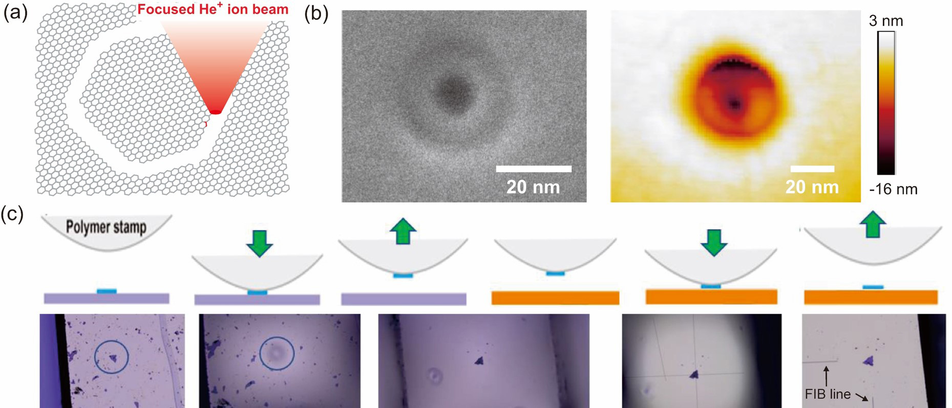
For the development of solid-state molecular machinery, a direct focused He+ beam machining is presented to fabricate solid-state nano-disk [1-3] (Fig. 1(a)) at the surface of a graphene multilayer micro-flake deposited on an Au/Ti/sapphire surface [2,3]. At irradiation doses larger than 5×10¹⁷ ions/cm2 and with a beam size well below 1 nm, graphene disks down to 20 nm in diameter have been machined with for nano-disk down to 30 nm in diameter, a central hole for preparing the positioning of a rotation axle (Fig. 1(b)). The local heat generated by this irradiation is inducing a partial graphene amorphization, melting, and deformation, leading to a complete graphene nano-disk vaporization at doses larger than 5×10¹⁸ ions/cm2 [3]. A dry transfer printing technique followed by a graphene surface cleaning was used to transfer the nano-disks from its initial surface to a fresh and clean surface [3] (Fig. 1(c)). Atomic force microscope was recorded to follow the vaporization as a function of the He+ dose to confirm the graphene solid-state nano-disk fabrication limit to about 20 nm with this process. Ultra-high vacuum scanning tunneling microscope was used to characterize the change in the electronic state by the local irradiation.

Fig. 1. (a) Schematic illustration of direct milling by a focused He+ ion beam. (b) Helium ion beam and AFM images of graphene nanodisk with a center hole. (c) Schematic illustration of graphene flake transfer process and corresponding optical microscope images at each transfer process.

Reference

  1. M. Sakurai, et al., Nanotechnology 31, 345708, (2020). DOI 10.1088/1361-6528/ab91f3
  2. M. Sakurai, et al., Vacuum 207, 111605, (2023). DOI 10.1016/j.vacuum.2022.111605
  3. M. Sakurai, et al., Nanotechnology 35, 315301, (2024). DOI 10.1088/1361-6528/ad40b5