Joint Workshop LANL/NIMS Quantum and Functional Materials and MANA International Symposium 2024
Quantum Materials - 01
Title
Synthesis of Large-Area GeS Thin Films on Insulator Substrates
Authors
Zhang Qinqiang, Matsumura Ryo, and Fukata Naoki
Affiliations
Nanostructured Semiconducting Materials Group, MANA, NIMS
URL
ZHANG.Qinqiang@nims.go.jp
Abstract
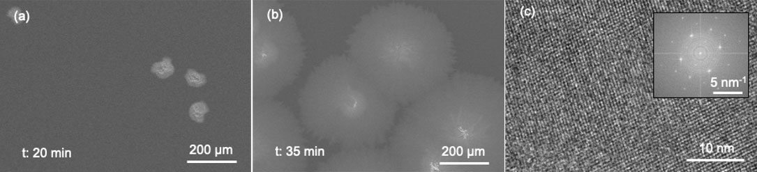
Germanium sulfide (GeS) is one of the potential two-dimensional layered semiconductors for development of next-generation electronics and optoelectronics. It has a direct bandgap of 1.6 eV and high mobility of 3680 cm2/Vs [1-2]. In this study, a novel method using pre-deposited amorphous GeS is applied to synthesis large-area GeS thin films on SiO2/Si substrates. The GeS powder is put in the vapor transport facility at a higher temperature and the SiO2/Si substrate is located at downstream area with a lower temperature to achieve the pre-deposited GeS layer. Scanning electron microscope images of synthesized GeS with different growth time of 20 and 35 min are shown in Figs. 1(a) and 2(b), respectively. Only bulk-like GeS clusters can be observed at 20 min. The synthesized GeS starts to show a thin-film-like structure at 35 min. The diameter of one GeS domain is around 400 µm. Fig. 1(c) shows the lattice fringe of transferred GeS thin films observed by transmission electron microscope. The selected area electron diffraction pattern with an aperture of about 200 nm is shown in the inset of Fig. 1(c) [3]. The succeed large-area GeS thin films express the significant potential to develop next-generation electronics and optoelectronic at the industrial level.
Reference
- E. Sutter et al., ACS Nano, 13(8), 9352-9362, (2019). DOI 10.1021/acsnano.9b03986
- F. Li et al., Journal of Materials Chemistry C 4(11), 2155-2159, (2016). DOI 10.1039/C6TC00454G
- Q. Zhang et al., ACS Applied Nano Materials 6(8), 6920-6928, (2023). DOI 10.1021/acsanm.3c00669