
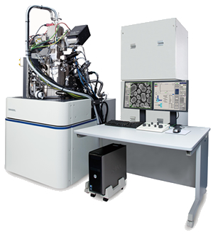
A28:FIB-SEMNanoGREEN Bldg. E-108

|
Maker |
Hitachi High-Tech Science |
|---|---|
|
Model |
SMF2000 |
|
Use for |
FIB processing, SEM/STEM observation, 3D image processing, EDS analysis, sample preparation for SEM/TEM. |
|
Outline |
The ion source of FIB is set perpendicular to the electron source of SEM. The specimen after FIB processing can be observed by SEM without moving the stage and 3D image acquired automatically. Low damage FIB processing is possible with a cryo-stage. Processing without air exposure is possible. |
Specification
FIB
|
Ion source |
Ga liquid metal ion source |
|---|---|
|
Accelerating voltages |
1,2,3kV 5 to 30 kV (in 5kV steps) |
|
Area of the observation field |
0.5 ㎛ x 0.5 ㎛ ~ φ2㎜ |
|
Image resolution |
4.0nm (at 30kV) |
|
Beam current |
Up to 90nA |
SEM
|
Electron source |
Thermal Field Emission gun(ZrO/W) |
|---|---|
|
Accelerating voltage |
0.1 to 30kV (in 10kV steps) |
|
Area of the observation field |
0.125 ㎛ x 0.125 ㎛ ~ 2㎜x2㎜(10kV) |
|
Image resolution |
1.1nm(at 20kV) 1.5nm(at 10kV) 2.5nm(at 1kV) for SEM |
|
Beam current |
Up to 10nA |
|
Detector |
STEM,BSE |
Low accelerating voltage Ar ion
|
Ion source |
Phillips Ionization Gauge(PIG) tpye ion source |
|---|---|
|
Accelerating voltages |
0.5 to 1kV |
|
Beam current |
Up to 10nA |
Other
|
Detectors |
EDS |
|---|---|
|
Specimen Holder |
The atmosphere blocking holder is available. |
Notice
- As this is an ultra-high vacuum instrument, samples containing volatile components that may contaminate the chamber cannot, in principle, be measured. Please consult us in advance regarding such samples. Samples containing sulfides cannot be measured.