
A16:GD-OESNanoGREEN Bldg. E-504

|
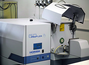
Maker |
HORIBA |
|---|---|
|
Model |
GD-Profiler 2 |
|
Use for |
Surface and depth analysis of the sample. |
|
Outline |
GD-OES allows the analysis of elemental depth profiles by optical detection of emissions from the excited atoms after Ar plasma sputtering. Low damage and high resolution measurements can be realized by pulsed sputtering. Surface analysis of electrically non-conductive samples is possible by high frequency glow discharge. Bulk quantification of solid materials is also possible. |
Specification
|
Detector |
Photo-multipliers |
|---|---|
|
Spectroscope |
Polychromator (32 elements), Monochromator (1 wavelength) |
|
Lower limit of detection |
few10 ppm~ |
|
Analysis Depth |
surface~200 ㎛ |
|
Depth resolution |
nm range |
|
Sample |
electrically conductive and non-conductive samples |
|
Spot diameter |
φ4㎜ |
Notice
- Non-conductive bulk samples cannot be measured.
- Layered samples with different conductivities are difficult to measure.