in a Transmission Electron Microscope (TEM-EELS)
-Review of our results-
Koji Kimoto and Yoshio Matsui
1. Introduction
2. High energy resolution using cold-FEG and deconvolution software.
3. Elemental & chemical analysis using ELNES.
4. Elemental & chemical mapping using Energy-Filtering TEM (EFTEM).
5. Spatially-resolved EELS for precise line analysis.
6. Bandgap measurement using monochromator.
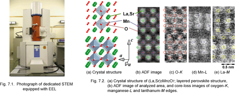
7. Atomic-column imaging using STEM-EELS (updated)
8. Delocalization in inelastic scattering (to be updated)
- Preservation of phase contrast in inleastic scattering.
- Coherence of core-loss electron
Dec. 3, 2005
Feb. 21, 2005
Oct. 18, 2003
Sep. 22, 2003
Electron energy-loss spectroscopy in a transmission electron microscope (TEM-EELS) is a powerful tool for analyzing the micro- and nano-structures of various materials. Elemental and chemical information is obtained with nanometer resolution using TEM-EELS. In this web page, we will show some of our results about material characterization. To get detailed information about TEM-EELS, the following textbooks are recommended.
[1.1] R. F. Egerton, Electron Energy-Loss Spectroscopy in the Electron Microscope 2nd ed. (Plenum Press, New York, 1996).
[1.2] L. Reimer, Energy-Filtering Transmission Electron Microscopy. (Springer-Verlag, Berlin, 1995).
[1.3] Z. L. Wang, Elastic and Inelastic Scattering in Electron Diffraction and Imaging. (Plenum Press, New York, 1995).
[1.4] R. Brydson, Electron Energy Loss Spectroscopy. (Springer Verlag, 2001).
[1.5] C. Colliex, "4.3.4. Electron energy-loss spectroscopy on solids" pp. 387-408 in International Tables for Crystallography C, 2nd ed.(Kluwer Academic Publishers, London, 1999)
2. High energy resolution using cold-FEG and deconvolution software.
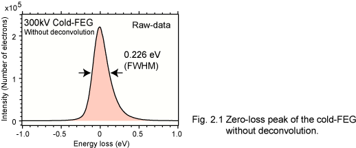
TEM-EELS is an effective way to obtain the chemical information, such as the valence and the coordination of specific atoms. High energy-resolution is required to observe energy-loss near-edge structures (ELNESs) for investigating the chemical bonding. The practical energy-resolution of EEL spectra mainly depends on (i) the energy spread of an electron source, (ii) EEL spectrometer aberration (i.e. non-isochromaticity), and (iii) instabilities in TEM high voltage and/or spectrometer power supply (i.e. energy-drift). We used 300 kV TEM (Hitachi, HF-3000) with an EEL spectrometer (Gatan, GIF 2002). The TEM is equipped with cold field-emission gun (cold-FEG). Firstly, we developed software for energy-drift correction [2.1]. It allows us to realize the inherent high energy resolution (~0.3 eV) of cold-FEG.
Recently we have applied a high-speed acquisiton technique 'streak-imaging', and a high energy-resolution of 0.23 eV is achieved without any deconvolution [2.3] (Fig. 2.1).
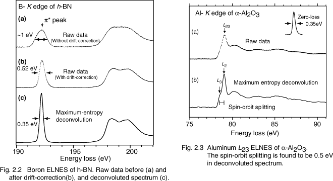
The energy spread of cold-FEG is narrower than that of other electron sources, such as a Schottky emission gun (~0.6 eV). It is, however, still larger than the intrinsic fine structures of EEL spectra. Therefore, a monochromator for an electron source or resolution-enhancement data processing is necessary. Dr. Ishizuka (HREM research Inc.) and we developed a software for the deconvolution using maximum-entropy (ME) algorithm and Richardson-Lucy (RL) algorithm. The energy-resolution of the deconvoluted spectrum becomes comparable to that obtained using a monochromator, whose energy-resolution is less than 0.2 eV [2.2]. (Fig. 2.2) Figure 2.3 shows an example of the ME resolution-enhancement in Al-L ELNES of alpha-Al2O3. The spin-orbit splitting (L3 and L2) is confirmed in a deconvoluted EEL spectrum.
[2.1] K. Kimoto and Y. Matsui, "Software techniques for EELS to realize about 0.3 eV energy resolution using 300 kV FEG-TEM", Journal of Microscopy, 208, 224 (2002).
[2.2] K. Kimoto, K. Ishizuka, T. Mizoguchi, I. Tanaka, and Y. Matsui, "The study of Al-L23 ELNES with resolution-enhancement software and first-principles calculation", Journal of Electron Microscopy, 52, 299 (2003). (Full text PDF is available, for personal use only)
[2.3] K. Kimoto, et al., "0.23 eV energy resolution obtained using a cold field-emission gun and a streak imaging technique", Micron, 36, 465-469 (2005).
3. Elemental & chemical analysis using ELNES
Fine structures in an electron energy-loss (EEL) spectrum originate in the transition from a core level to unoccupied states under the dipole selection rule, therefore energy-loss near edge structure (ELNES) includes the detailed information of a electronic structure of a material. The fingerprint method, in which an observed spectrum is compared with several spectra of known materials, is simple and effective for the interpretation of ELNES.
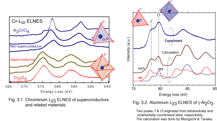
Figure 3.1 shows Cr-L ELNES in cupper-oxide superconductors and related materials. The ELNESs suggest that chromium is CrO6 (III) octahedron in the superconductors and is CrO4 (VI) in the related materials. The valence of Cr is important in terms of materials science, because it directly relates to the hole doping, which is critical for cupper-oxide superconductors. [3.1]
Although the fingerprint technique is very useful, appropriate standard spectra are not always prepared. By contrast, first-principles ELNES calculation is available if the atom coordinates of the material are known. Recent advanced first-principles calculation methods successfully reproduce experimental results, providing a detailed interpretation.
Figure 3.2 shows the Al-L ELNES of gamma-Al2O3. In gamma-Al2O3, Al atoms are tetrahedrally and octahedrally coordinated (i.e., AlO4 and AlO6). We calculated two spectra, in which tetrahedrally and octahedrally coordinated aluminum atoms are excited. These sophisticated calculations are performed by Dr. Mizoguchi and Prof. I. Tanaka of Kyoto University using OLCAO method [3.2]. The calculation results successfully reproduce experimental results, and the origins of two peaks near the threshold are identified.
We have studied a variety of materials using ELNES and its first-principles calculation; cubic (spinel)-Si3N4 [3.3], Al2O3 [3.2], oxycarbonate superconductors [3.4] and SiOxNy [3.5].
[3.1] Y. Anan, T. Asaka, H. Kurami et al., Physica C 357-360, 371 (2001).
[3.2] K. Kimoto, K. Ishizuka, T. Mizoguchi et al., Journal of Electron Microscopy 52, 299 (2003).
[3.3] I. Tanaka, T. Mizoguchi, T. Sekine et al., Applied Physics Letters 78, 2134 (2001).
[3.4] K. Kimoto, Y. Anan, T. Asaka et al., Journal of Electron Microscopy 50, 307 (2001).
[3.5] K. Kimoto, K. Kobayashi, T. Aoyama et al., Micron 30, 121 (1999).
4. Elemental & chemical mapping using energy-filtering TEM (EFTEM)
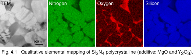
One of the major applications of the energy-filtering TEM (EFTEM) is elemental mapping. Two-dimensional elemental maps can be observed using a few energy-filtered images of core-loss electrons. Figure 4.1 shows one of the typical demonstrations of EFTEM elemental mapping. The specimen is a polycrystalline Si3N4 with a small amount of Y2O3 and MgO. Silicon, nitrogen and oxygen elemental maps are easily observed [4.1] using two-window method [1.1].
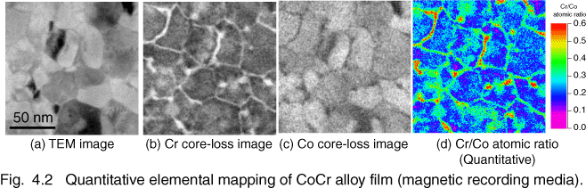
Although Fig. 4.1 is qualitative elemental mapping, quantitative elemental mapping is also possible. Figure 4.2 shows the quantitative elemental mapping of a CoCrTa film, which is used for magnetic recording media. We observe Cr and Co core-loss images using three-window method ((b) & (d)), then construct the quantitative atomic-ratio map of Cr/Co (d). It shows the compositional inhomogeneity, in which chromium is accumulated at grain boundaries. We have observed a variety of CoCr alloy films for magnetic recording media, such as CoCrTa and CoCrPt. It is found that magnetic properties directly depend on the compositional inhomogeneity of the CoCr films [4.2] [4.3] [4.4] [4.5].
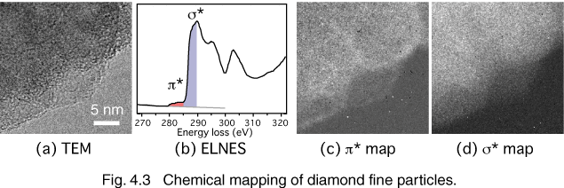
An energy-loss spectrum includes chemical bonding information, therefore the chemical analysis can also be performed. We observed the microstructure of diamond particles formed by CVD (chemical vapor deposition). Figure 4.3 (a) shows the TEM image of the diamond particles. The diameter of the diamond particle is a few hundred nm, but the particle consists of smaller sub-grains of approximately 20-50 nm in diameter. The carbon K-edge EEL spectrum of the whole area (b) shows not only sigma* but also pi* peak, which is originated from sp2 bonding. We observe pi* and sigma* maps ((c) & (d)) to investigate chemical boding of the specimen. It is found that the grain boundaries and the surface of the sub-grain have sp2 bonding. This gives us useful information in controlling the grain size of nanocrystalline diamond particles and in optimizing the growth conditions in the CVD process [4.6].
[4.1] K. Kimoto and Mitomo, Unpublished work (2001).
[4.2] K. Kimoto, Y. Yahisa, T. Hirano et al., Jpn. J. Appl. Phys. 34, L352 (1995).
[4.3] Y. Yahisa, K. Kimoto, K. Usami et al., IEEE Transactions on Magnetics 31, 2836 (1995).
[4.4] Y. Hirayama, K. Kimoto, and M. Futamoto, IEEE Transactions on Magnetics 32, 3807 (1996).
[4.5] K. Kimoto, Y. Hirayama, and M. Futamoto, Journal of Magnetism and Magnetic Materials 159, 401 (1996).
[4.6] K. Okada, K. Kimoto, S. Komatsu et al., Journal of Applied Physics 93, 3120 (2003).
5. Spatially-resolved EELS for precise line analyis.
Spatially-resolved EELS technique is the method to acquire plural spectra at different positions, simultaneously. The point of this technique is the usage of a line-focus energy filter. It should be mentioned that a few authors successfully applied this approach in the 50's as angular-resolved EELS [5.1]. Recently a few authors apply this kind technique as 'laterally-resolved EELS' [5.2] or 'spectrum-profiling' [5.3].
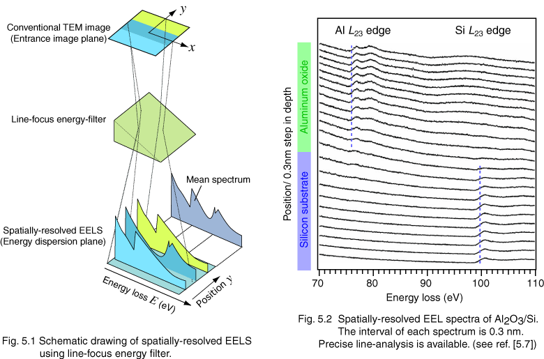
Figure 1 shows the schematic diagram of spatially-resolved EELS technique. A conventional (unfiltered) TEM image is projected on the entrance image plane of a line-focus energy filter. Using the line-focus energy filter, a TEM image of certain energy is focused as a line on the energy dispersion plane, and a band-shaped spectrum is projected; axis x and axis y in the band-shaped spectrum correspond to the energy-loss and the position y in the TEM image, respectively. We term the band-shaped spectrum as spatially-resolved (EEL) spectrum. As shown in Fig. 5.1, we can obtain many spectra at different positions along axis y as a single spatially-resolved spectrum. It is practically effective to detect the differences in energy-loss near edge structure (ELNES) because plural spectra are acquired simultaneously. For example, a small chemical shift of less than 0.5 eV can be evaluated by this method.
We applied this technique since 1997 to dielectric materials for semiconductor devises, such as Si3N4/SiO2/Si [5.4][5.5][5.6] and high-k materials [5.7]. Figure 5.2 shows the application data of spatially-resolved EELS for Al2O3 thin film on Si substrate. EEL spectra are measured at 0.3 nm interval. We also applied this technique to a perovskite superlattice, in which two Ti atomic-layers are clearly observed.
This method is also effective for elucidating the coherence of inelastically scattered electrons [5.9][5.10]
[5.1] H. Watanabe: Journal of the Physical Society of Japan 11 (1956) 112.
[5.2] T. Walther: Ultramicrosc. 96 (2003) 401.
[5.3] U. Golla-Schindler,et al.: Ultramicrosc. 96 (2003) 573.
[5.4] K. Kimoto, et al.: Chemical Shift Mapping of Si L and K edges Using Spatially Resolved EELS and Energy-Filtering TEM. Journal of Electron Microscopy 46 (1997) 369.
[5.5] T. Sekiguchi, K. Kimoto, T. Aoyama, Y. Mitsui: Nitrogen Distribution and Chemical Bonding State Analysis in Oxynitride Film by Spatially Resolved Electron Energy Loss Spectroscopy (EELS). Jpn. J. Appl. Phys. 37 (1998) L694.
[5.6] K. Kimoto, et al.: Analyses of composition and chemical shift of Si oxynitride film using EF-TEM based spatially resolved EELS. Micron 30 (1999) 121.
[5.7] K. Kimoto, Y. Matsui, T. Nabatame, T. Yasuda, T. Mizoguchi, I. Tanaka: Coordination and interface analysis of atomic-layer-deposition Al2O3 on Si(001) using energy-loss near-edge structure. Appl. Phys. Lett. 83 (2003) 4306.
[5.8] K. Kimoto, Y. Matsui, H. Yamada, M. Kawasaki, X. Yu, Y. Kaneko, and Y. Tokura, "Atomic-scale characterization of perovskite superlattice using chemical lattice imaging and spatially resolved electron energy-loss spectroscopy", Appl. Phys. Lett., vol. 84, pp. 5374-5376, (2004).
[5.9] K. Kimoto, Y. Matsui: The Fourier images feature of the lattice fringes formed by low-loss electrons as observed using spatially-resolved EELS technique. Journal of Electron Microscopy 50 (2001) 377.
[5.10] K. Kimoto, Y. Matsui: Experimental investigation of phase contrast formed by inelastically scattered electrons. Ultramicrosc. 96 (2003) 335.
6. Bandgap measurement using monochromator.
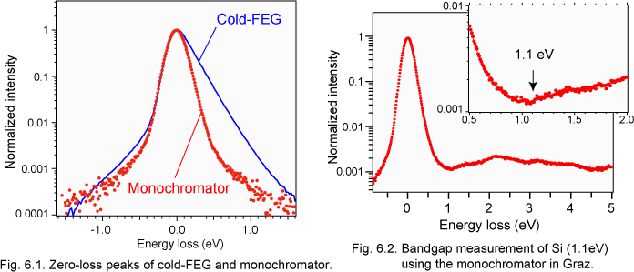
Monochromators for transmission electron microscopy (TEM) are now commercially available. The energy spread of the monochromator is reported to be 0.1 - 0.25 eV in full-width at half-maximum (FWHM). However, as abovementioned, the energy spread of a cold field-emission electron gun (CFEG) is less than 0.3 eV [6.1], and the spread can be deconvoluted by advanced softwares [6.2]. What is the advantage of the monochromator? One of the advantages of the monochromator exists in bandgap measurement. Figure 6.1 shows the comparison of the zero-loss peak (ZLP) of a CFEG and the monochromator. The FWHM of the monochromator is not so narrow (0.23 eV), but the intensity of its tail is relatively low in comparison with that of CFEG. This low-intensity tail allows us to measure the onset of low-loss intensity without a numerical process. Figure 6.2 shows the example of bandgap measurement. The bandgap of Si (1.12eV) is confirmed as the onset of the signal [6.3]. The monochromator result was obtained in FELMI-TU Graz (Graz University of Technology) by Drs. Kothleitner, Grogger and Prof. Hofer.
[6.1] K. Kimoto and Y. Matsui, Journal of Microscopy, vol. 208, pp. 224-228, (2002).
[6.2] K. Kimoto et al., Journal of Electron Microscopy, vol. 52, pp. 299-303, (2003). (Full text PDF file is available, for personal use only)
[6.3] K. Kimoto, G. Kothleitner, W. Grogger, Y. Matsui, and F. Hofer, "Advantages of a monochromator for bandgap measurements using electron energy-loss spectroscopy", Micron, vol. 36, pp. 185-189, (2005).
7. Atomic-column imaging using STEM-EELS (updated, but is still under construction).
A combination of scanning transmission electron microscopy (STEM) and electron energy-loss spectroscopy (EELS), i.e., spectrum-imaging [7.1], is a promising technique for high-spatial-resolution analysis. We have successfully demonstrated element-selective atomic-column imaging using stabilized STEM instrument [7.2] and EELS. The atomic columns of La, Mn and O in the layered manganite La1.2Sr1.8Mn2O7 have been visualized as two-dimensional images [7.3] . The delocalization in inelastic scattering is one of the decisive factors to realize the atomic-column imaging. (to be continued...) [7.4]
[7.1] C. Jeanguillame and C. Colliex, Ultramicrosc. 28 (1989) 252-257.
[7.2] K. Kimoto, et al., "Development of dedicated STEM with high stability". J. Electron Microsc. 56 (2007) 17-20.
[7.3] K. Kimoto, et al., "Element-selective imaging of atomic columns in a crystal using STEM and EELS" Nature (2007).
[7.4] K. Kimoto, et al., "Decisive factors for realizing atomic-column resolution using STEM and EELS" Micron (2007).
[7.5] We thank Prof. Y. Tokura and Dr. T. Kimura for providing the manganite specimen. We thank Prof. R. F. Egerton, Dr. M. Malac, Dr. K. Suenaga and Prof. H. Kurata for discussions and encouragement. We also thank Drs. M. Barfels, M. Kundmann and J. Hunt (Gatan) for their cooperation in the installation of an EEL spectrometer, and Dr. T. Yokosawa (NIMS), Drs. K. Nakamura, S. Aizawa and S. Isakozawa (Hitachi High-Technologies) for their cooperation in developing the STEM.
Acknowledgements
The authors express thanks to coworkers in NIMS. The author (KK) thanks to Drs. Usami, Hirano, Narishige, Yahisa, Hoshiya, Sekiguchi, Aoyama, Kozono, Futamoto, Hirayama of Hitachi Ltd, and Drs. Isakozawa, Tomita, Taniguchi, Inada, H. Tanaka, Taya, Y. Sato and K. Saito of Hitachi high-technologies. The authors also thank to Dr. Ishizuka of HREM Research Inc., Prof. I. Tanaka & Dr. Mizoguchi of Kyoto University, Prof. N. Tanaka of Nagoya University, and Prof. M. Tanaka of Tohoku University.