


Transmission Electron Microscopes
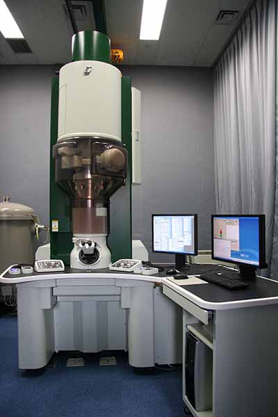
- JEM-ARM200F-G
Real working environment physical characterization TEM This microscope has TEM image and STEM probe aberration correctors for high-resolution observations. Furthermore, it enables us to do in-situ observation, chemical analysis and potential measurement under various conditions by utilizing specimen holders.
・Acceleration voltage: 80, 120, 200 kV
・TEM, STEM, EDS, EELS, electron holography,
3D imaging and in-situ observations (high temperature (up to 1200℃), low temperature (up to -160℃), a gas environment, illumination, bias application etc.) 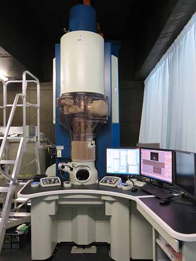
- JEM-ARM200F-B
Real working environmental electron holography microscope This microscope has TEM image and STEM probe aberration correctors for high-resolution observations. It is capable of in-situ observation, chemical analysis and potential measurement under various conditions by utilizing specimen holders. Cold FEG enables high-resolution STEM even at low acc. Volts
・Acceleration voltage: 60, 80, 200 kV
・TEM, STEM, EDS, EELS, electron holography, and in-situ observations (high temperature up to 1200℃, a gas environment, bias application etc.) 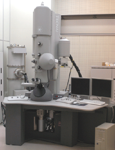
- FEI Tecnai G2 F30
300 kV transmission electron microscope This is a 300 kV transmission electron microscope equipped with field emission gun, TEM, STEM, EDS, energy filter (GIF) and Lorentz microscopy are performed. 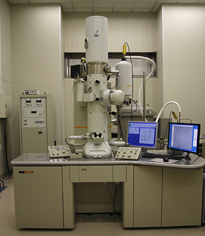
- JEM-2100F1, JEM-2100F2
200 kV field emission TEM The microscope has a user-friendly operation interface. It supports the following modes: TEM, STEM, EELS, EDS, NBD and CBED. Three-dimensional observation is possible with a dedicated holder and tomography software. 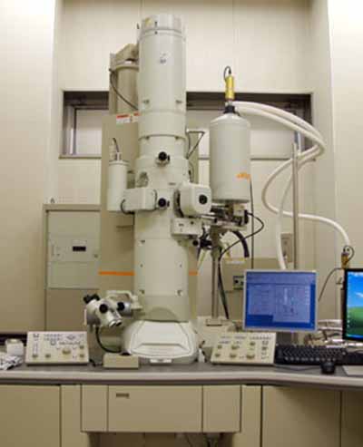
- JEM-2100
200 kV transmission electron microscope This is a user-friendly 200 kV transmission electron microscopy with LaB6 Thermal emission gun. It supports TEM and EDS (point analysis) mode. It is also equipped with CCD camera for diffraction pattern. 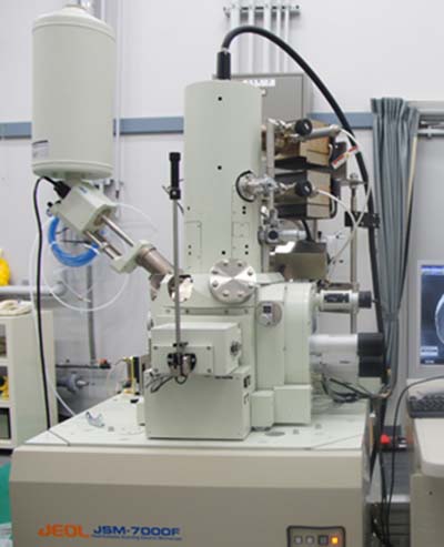
- JSM-7000F
Field emission gun scanning electron microscope This scanning electron microscope (SEM) is equipped with a thermal field-emission gun (FEG). EDS for elemental analysis and mapping is possible. Various sample sizes and various kinds of materials are acceptable.
Acceleration Voltage: 0.5~30 kV 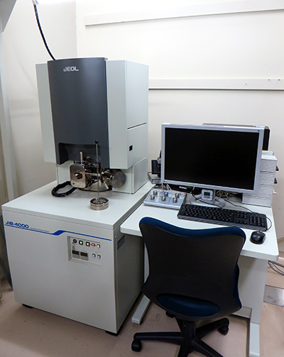
- JIB-4000
FIB (Focused ion beam) specimen preparation system A facility with which a TEM thin film specimen can be directly cut and picked-up from a bulk material. A specimen can be made from an interesting place in an accuracy of sub-micrometer.
A membrane that has been ion milled and separated out of the bulk inside the FIB in advance can be carried and bonded on the TEM mesh using the Pick-Up-System. 
- JEM-9320FIB
FIB (Focused ion beam) specimen preparation system An apparatus with which a TEM thin film specimen can be directly cut and picked-up from a bulk material. A specimen can be made from an interesting place in an accuracy of sub-micrometer.
A membrane that has been ion milled and separated out of the bulk inside the FIB in advance can be carried and bonded on the TEM mesh using the Pick-Up-System. 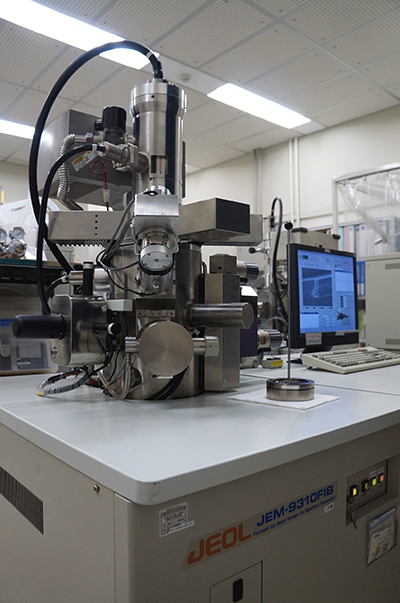
- JEM-9310FIB1, JEM-9310FIB2
FIB (Focused ion beam) specimen preparation system A facility with which a TEM thin film specimen can be directly cut and picked-up from a bulk material. A specimen can be made from an interesting place in an accuracy of sub-micrometer.
A membrane that has been ion milled and separated out of the bulk inside the FIB in advance can be carried and bonded on the TEM mesh using the Pick-Up-System. 
- Pick-up System
Pick-up of FIB-processed sample
A common-use facility in Sengen site
(Room 115, Physical Analysis Laboratory at Sengen)
- NB5000
Dual beam system An instrument equipped with focused ion beam (FIB) fabrication and scanning electron microscopy (SEM) functions. SEM observation of a part where is fabricated by FIB is possible. Furthermore, the fabricated piece can be micro-sampled inside the column.
- TEM sample preparation apparatus There are tools for cutting, mechanical polishing, chemical-mechanical polishing (CMP), embedding, staining, etc. Cross-sections, damage-free wedges, low temperature and low energy ion milled and biological samples can be prepared.
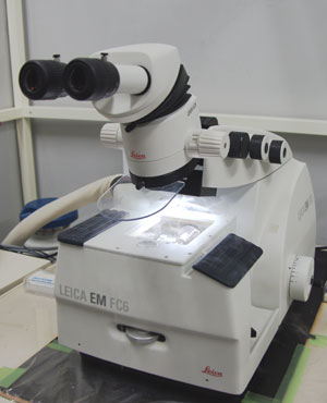
- Leica EM UC6
Ultramicrotome This ultramicrotome allows preparation of ultrathin sections of soft materials with smooth surfaces such as biological and polymer samples for TEM. Glass and diamond knives are available. Sample cooling to liquid nitrogen temperature is possible (cryo-microtome). 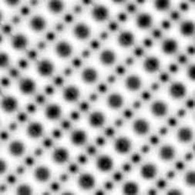
- HRTEM Analysis System
HRTEM simulation/ Crystal modelling
Tools for TEM image processing, FFT, Crystal modelling and HRTEM simulation
-
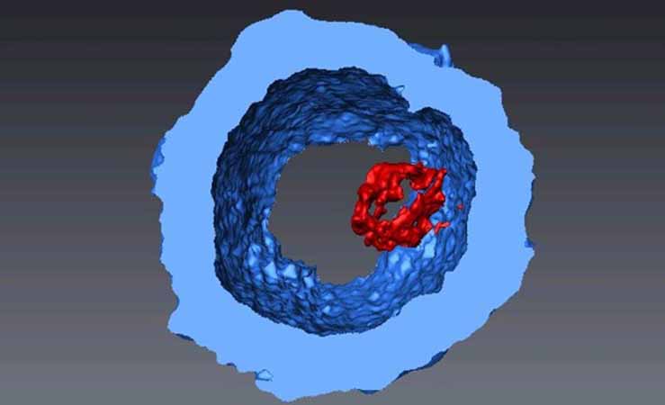
- Electron tomography analysis system
3D analysis tools
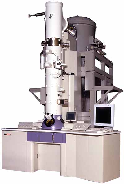
- JEM-3100FEF
Atom-discriminating electron microscope Equipped with an OMEGA-type energy filter, this microscope allows high-resolution mapping of chemical composition.
・Imaging resolution: 0.17 nm
・Spatial resolution of chemical analysis: 0.5 nm
・EDS, EELS analysis 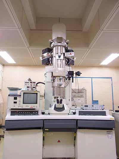
- HF-3000L
Cold-FEG Lorentz Electron Microscope It is possible to observe Lorentz images at various temperatures using dedicated sample holders.
・Acceleration voltage: 300 kV, 200 kV, 100 kV
・Spatial resolution: 1.5 nm (at 300 kV) 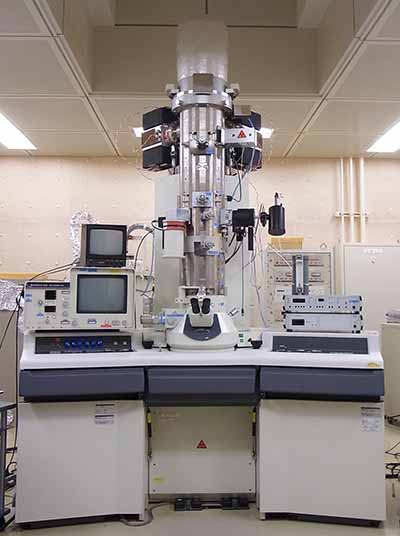
- HF-3000S
Cold-FEG Transmission Electron Microscope This cold-FEG transmission electron microscope is equipped with an energy filter and low-temperature specimen holders.
・Acceleration voltage: 300 kV, 200 kV, 100 kV
・Spatial resolution: 0.2 nm (at 300 kV)
・Energy resolution: 0.3 eV (at 300 kV) 
- FEI Titan Cubed
Atomic-resolution analytical electron microscope It allows to observe TEM/STEM images with the world’s top spatial resolution, owing to aberration correctors at the illumination and imaging lens systems. The microscope is equipped with a monochromated electron gun and supports EELS measurements with a high energy resolution.
-Acceleration voltage: 300 kV, 80 kV
-TEM spatial resolution: 90 pm (at 80 kV)
-STEM spatial resolution: 60 pm (at 300 kV)
-Energy resolution: 70 meV (at 80 kV) 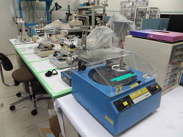
- Ceramics sample preparation facilities
TEM-specimen preparation apparatuses consist of cutters, mechanical grinders,
dimple grinders and ion milling systems. It is possible to obtain thin samples of
ceramics and semiconductors suitable for TEM/STEM observation.
・Dimpling
・Ion milling (5 kV; in situ observation by a CCD camera; sample cooling)
・Low-voltage ion milling (0.2 ~ 2 kV)
Detail 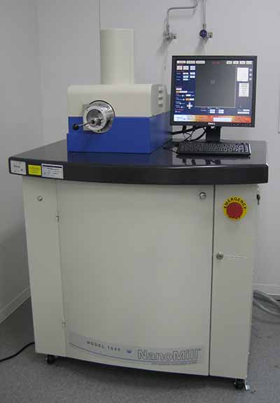
- NanoMill Model1040
Damage-free TEM Sample Milling Apparatus This Ar- ion milling apparatus uses ion energies ten times lower than in conventional systems. The sample is imaged using secondary electrons induced by the Ar ion beam.