- Precise LT-STM Active Nano-Characterization -
Fig.1
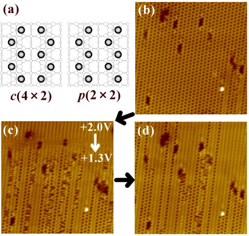
Phase Manipulation between c(4x2) and p(2x2) on Si(100) Surface at 4.2K
- Precise LT-STM Active Nano-Characterization -
Fig.1
| (a): Top view of the Si(100) surface reconstruction of c(4x2) and p(2x2) (b)-(d): A sequence of c(4x2)/p(2x2) transition observed in the empty state images of the n-type Si(100) surface at 4.2 K. (b): Initial c(4x2) dominant surface aquired at a sample bias voltage of +1.3 V, then the bias voltage was gradually decreased to +1.3 V during the scan. (c): The surface of a large area of p(2x2) recorded at +1.3 V post transition. All images were recorded with a tunneling current of 30 pA. |