- Home
- > Research
- > Research Highlights
- > Vol. 78 New Diamond Transistor Exhibit・・・
 Research Highlights
[Vol. 78]
New Diamond Transistor Exhibits High Hole Mobility
- Previous
- Index
- Next
29 Jul, 2022
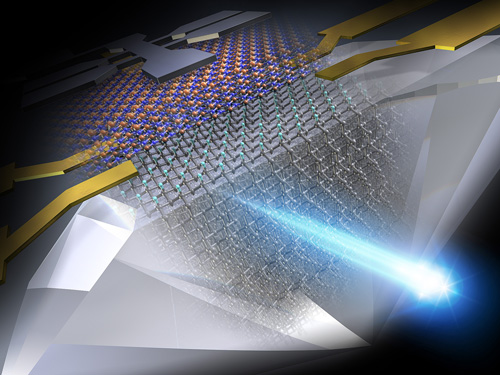
A research team at MANA, using a new fabrication technique, has developed a diamond field-effect transistor with high hole mobility, which can lead to reduced conduction loss and higher operational speeds.

Field-effect transistors (FETs) are semiconductor devices that can switch electric power and amplify electric signals. FETs made of wide-bandgap semiconductors can handle high power efficiently and are useful for power electronics and communications. The use of SiC and GaN is therefore growing, but diamond has a wider bandgap and more desirable properties that could boost device performance.
The team used a new fabrication technique to develop the FET, wherein it fabricated the transistor with hexagonal boron nitride as a gate insulator and without exposing the diamond’s surface to air. The advantage is that it can reduce the density of negative charges on the diamond surface. If there are negative charges, they produce random Coulomb potential, which scatters the holes when they conduct near the diamond surface. This degrades the effectiveness of hole conduction and decreases the mobility of the holes.
Also, with the negative charges, even if no gate voltage is applied, there are holes, and so the transistor is "normally on," and this is not suitable for power electronics applications.
"In contrast, in our new technique, we can reduce the density of negative charges on the diamond surface. So the holes are less scattered, and therefore we can obtain higher mobility," said team leader Dr. Takahide Yamaguchi. "This also results in 'normally-off’ operation, which is desirable for power electronics."
Dr. Yamaguchi pointed to some possible applications of this breakthrough. "Our new approach for fabricating diamond transistors could be used to make low-loss switches for power electronics and high-frequency high-output amplifiers for communications."
This research was conducted by Yosuke Sasama (NIMS Postdoctoral Researcher, Surface Quantum Phase Materials Group, WPI-MANA, NIMS), Takahide Yamaguchi (Principal Researcher, Surface Quantum Phase Materials Group, WPI-MANA, NIMS) and their collaborators.
Reference
“High-mobility p-channel wide-bandgap transistors based on hydrogen-terminated diamond/hexagonal boron nitride heterostuctures”
Yosuke Sasama, Takahide Yamaguchi, et al.
Journal: Nature Electronics, 5, 37-44 (23 December 2021)
DOI : s41928-021-00689-4
Yosuke Sasama, Takahide Yamaguchi, et al.
Journal: Nature Electronics, 5, 37-44 (23 December 2021)
DOI : s41928-021-00689-4
Affiliations
International Center for Materials Nanoarchitectonics (WPI-MANA), National Institute for Materials Science (NIMS), Namiki 1-1, Tsukuba, Ibaraki 305-0044, Japan
Contact information
Research Center for Materials Nanoarchitectonics (MANA)
National Institute for Materials Science
1-1 Namiki, Tsukuba, Ibaraki 305-0044 Japan
Phone: +81-29-860-4710
E-mail: mana-pr[AT]nims.go.jp
1-1 Namiki, Tsukuba, Ibaraki 305-0044 Japan
Phone: +81-29-860-4710
E-mail: mana-pr[AT]nims.go.jp