- Home
- > Research
- > Research Highlights
- > Vol. 77 New TEM Technique Creates 2.8n・・・
 Research Highlights
[Vol. 77]
New TEM Technique Creates 2.8nm Transistor
An international research team at MANA has used a transmission electron microscope (TEM) to create a 2.8nm transistor consisting of nanochannels embedded in metallic carbon nanotubes (CNTs), which exhibits quantum transport at room temperature.
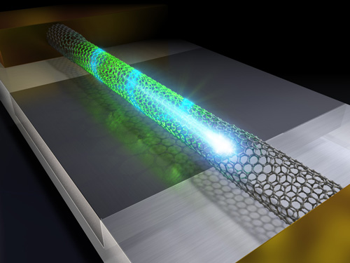
One major aim of nanotechnology research is to control the helical structure of a CNT. This structure determines the nanotube’s properties, and altering it can result in drastic changes, such as turning it from a metal to a semiconductor. To achieve this, the focus has been on growing nanotubes to control the structure, but this has been very difficult due to their extremely small size, only one or two nanometers in diameter.
To address this difficulty, researchers at MANA have developed a technique to precisely manipulate individual CNTs and alter their helical structure inside a TEM.
The MANA team used nanoprobes to apply tension and heat to the CNT. This deformed a section of the nanotube, altering its structure and changing it from a metal into a semiconductor.
The section of the altered nanotube was very short, and formed a semiconductor embedded in a metallic nanotube. The researchers believe this can be used as a semiconductor channel, and with the original metallic nanotube as the source and drain, the effect is like a molecular transistor embedded inside the nanotube.
Dr. Dai-Ming Tang, leading member of the team, said, "This transistor is extremely small, only 2.8nm in channel length, shorter than any current silicon-based transistors. In fact, this is among the world’s smallest transistors, and we created it by using our new technique."
Another exciting aspect of this work relates to the behavior of materials on such tiny scales. "Because we can make such a very small transistor, other effects appear," Dr. Tang said. "For example, we have seen quantum transport at room temperature, which is usually observed only at extremely low temperatures."
This could allow the density of transistors on a computer chip to be much higher, leading to more powerful and faster electronics.
This research was conducted by Daiming Tang (Senior Researcher, Functional Nanomaterials Group, WPI-MANA, NIMS) and his collaborators.
Reference
“Semiconductor nanochannels in metallic carbon nanotubes by thermomechanical chirality alteration”
Dai-Ming Tang et al.
Journal: Science, 374, 1616-1620 (24 December 2021)
DOI : 10.1126/science.abi8884
Dai-Ming Tang et al.
Journal: Science, 374, 1616-1620 (24 December 2021)
DOI : 10.1126/science.abi8884
Affiliations
International Center for Materials Nanoarchitectonics (WPI-MANA), National Institute for Materials Science (NIMS), Namiki 1-1, Tsukuba, Ibaraki 305-0044, Japan
Contact information
Research Center for Materials Nanoarchitectonics (MANA)
National Institute for Materials Science
1-1 Namiki, Tsukuba, Ibaraki 305-0044 Japan
Phone: +81-29-860-4710
E-mail: mana-pr[AT]nims.go.jp
1-1 Namiki, Tsukuba, Ibaraki 305-0044 Japan
Phone: +81-29-860-4710
E-mail: mana-pr[AT]nims.go.jp