


Summer Science Camp 2012 was successfully held
August 3, 2012
Summer Science Camp 2012 sponsored by JST was held at MANA for 3 days on August 3-5. The 10 participating high school students from all over Japan attended 3 practice and observation sessions related to nanotechnology.
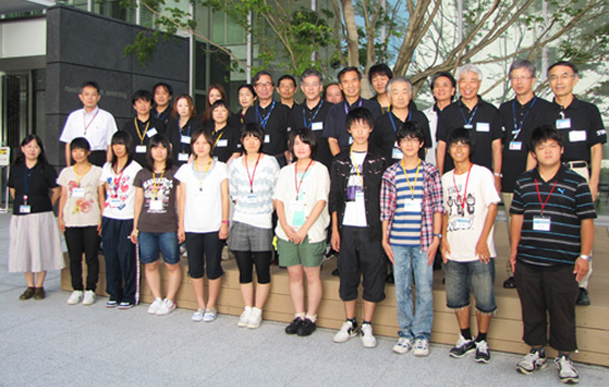
Group photo of the participants and instructors.
Observation of the nano-scale world
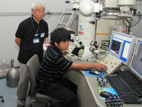
Fine structure observation by Scanning Electronic Microscope (SEM)
After receiving a basic lecture about SEM, the participants observed various kinds of fine structures by SEM, including the head and a leg of an insect, different crystals, and carbon nanotube wires. They learned that nano-scale observation requires a focused beam of high-energy electrons, which has shorter wavelength than light.
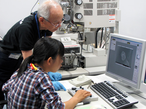
A participant operates SEM.
Taking a SEM image of butterfly scales.
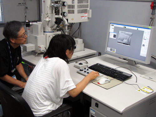
Atomic scale observation by Transmission Electron Microscope (TEM)
After receiving an introduction about TEM, the participants observed a semiconductor chip with atomic scale. They also verified what kinds of elements are composed in a specific area of the chip by Energy Dispersive X-ray spectroscopy (EDX) measurement.
Explanation about EDX measurement.
A participant operates TEM to take a photo image of a crystal lattice.
Working inside the clean room
Learning lithography
Inside the clean room, the participants experienced two kinds of photolithography including a “positive-type process” and a “negative-type process” to learn about semiconductor manufacturing. To observe the difference between the two types of processes, the participants checked and compared the results under the microscope.
Then they used photolithography to make two types of Au-electrode wires with and without dust to verify the sensitivity to environmental contamination. By I-V measurements and SEM observation of the electrode structure, the participants learned that even a single nano-scale dust can cause short-circuit in an electrode, which is the reason why semiconductor processing needs an environment with a controlled level of contamination.
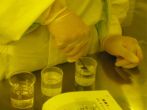
Carefully rinsing a chip with water.
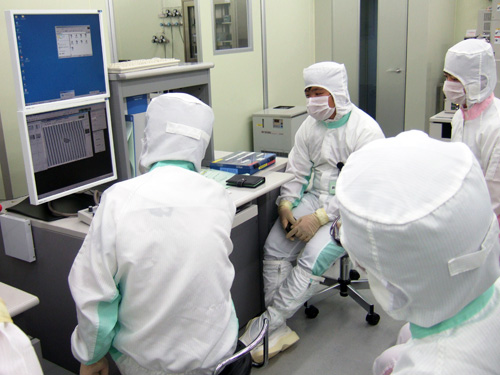
Verifying the sensitivity of an electrode to contamination.
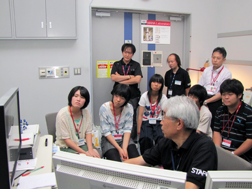
Presentinon of the results
On the last day of the program, the participants were divided into two groups and presented their results obtained during three days. The participants then had to response to questions and comments from the instructors before they received the well-deserved certificate of the Summer Science Camp from MANA Director-General Dr. Masakazu Aono.
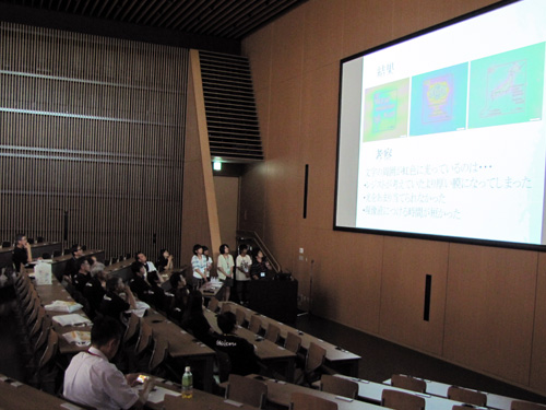
Presentation by group A.
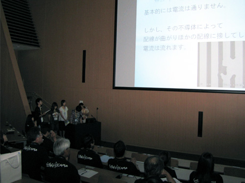
Presentation by group B.
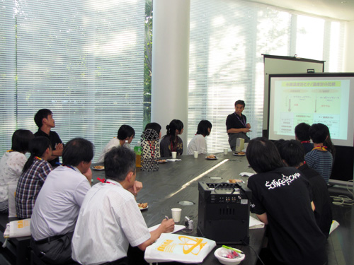
Other lecture and a reception
After finishing the SEM program on the first day, the participants enjoyed to listen to a lecture entitled “Nobel Prize and Serendipity” by MANA COO Dr. Yoshio Bando. Then the participants had a pleasant chat with the instructors and young researchers at the MANA reception party.
A lecture by Dr. Yoshio Bando.
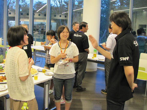
A young researcher answers to a question of a participant.