Quantum Materials Field
Nanostructured Semiconducting Materials Group
New functional semiconductor nanodevices using novel physical properties
Group Leader: Naoki Fukata
Next-Generation Semiconductor, Nanostructures and devices
Current Topics
Ge is noticed as a next generation semiconductor material in both electronic and optical devices. However, since Ge is an indirect semiconductor, there is a problem in its application to light emitting devices. In this study, pseudo direct transition emission was enabled in Ge by (1) carrier induction at point by high concentration n-type impurity doping and (2) valence band degeneracy by high tensile strain induction due to CW laser annealing. Furthermore, the highest carrier concentration in Ge thin film formed on insulating substrate was achieved by (3) enabling direct transition even with Sn addition, and (4) greatly improving Sb activation by introducing Si.
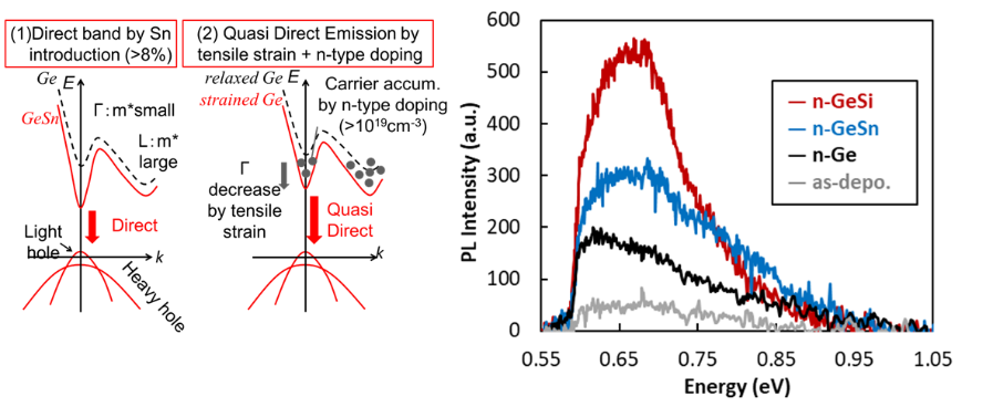
Fig. 1. Direct bandgap transformation and quasi-direct bandgap Ge with tensile strain and n-type doping. l. Photoluminescence (PL) spectra of crystallized n-GeSi, n-GeSn, and n-Ge.
Outline of Research
Nanostructures such as quantum dots (QDs), nanowires (NWs) and nanosheets (NSs) give novel function and new device application. As a material, attention is paid to group IV semiconductor materials such as C, Si and Ge. By functionalizing them we explore new electrical and optical devices such as high-mobility/low energy consumption transistors, high-efficiency enery-related devices and new device applications using quantum nanomaterials and quantum phenomena (Figure 2).
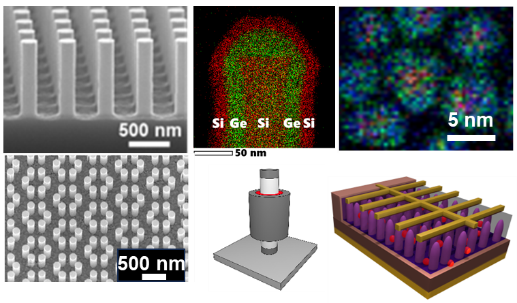
Fig. 2. (a-d) SEM and EDX images of NWs and QDs using semiconductor materials and their new application for transistor and photovoltaic devices.
References
- R. H. Saputro et al., ACS Appl. Electron. Mater. 6, 4297 (2024). DOI: 10.1021/acsaelm.4c00399
Group members
-
 Naoki Fukata・Group Leader・Field Director of Quantum Materials Field
 -
 Wipakorn Jevasuwan・Senior Researcher
 -
 Ryo Matsumura・Researcher
Activities
-
Feb 27, 2024Ryo Matsumura, Senior Researcher, Receives the "MRM Poster Award 2023"