Independent Researcher
Takayuki Harada
We search for new phenomena and functionality in thin-film heterostructures.
Exploring thin-film heterostructures for fundamental science and electronic applications
Current Topics
The current focus is the application of the metallic delafossites in advanced interconnects. As the miniaturization of logic circuits, Cu interconnects are facing serious increase of resistivity in future technology nodes. To overcome this issue, search for an alternative interconnect material is crucial. Recently, metallic delafossites are theoretically proposed as an interconnect candidate that has better scaling behavior because of quasi-two dimensionality. Based on the scalable thin-film growth techniques, we are trying to integrate the metallic delafossites with semiconductor devices.
Outline of Research
We have developed thin films of layered oxides that are as conductive as elemental gold (Fig. 1). Having quasi two-dimensional electronic states, the thin films of metallic delafossites are expected to maintain the high conductivity when scaled down to a few nanometer thicknesses. We are exploring application in electronics, while searching for quantum transport phenomena that arises from the high-density mobile quasi two-dimensional electrons.
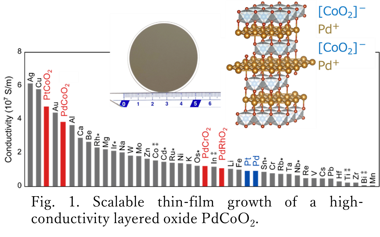
Fig. 1. Scalable thin-film growth of a high-conductivity layered oxide PdCoO2.
References
- T. Harada and Y. Okada, APL Mater. 10, 070902 (2022) DOI: 10.1063/5.0097269
- T. Harada, T. Nagai, M. Oishi, Y. Masahiro, J. Appl. Phys. 133, 085302 (2023)
DOI: 10.1063/5.0136749
Group members
-
 Takayuki Harada・Independent Researcher・ElectroActive Materials Team
Activities
-
Jan. 23 2024Independent Scientist Appears in Media for His Research Achievement
-
Feb.26 2024Students from La Trobe University in Australia and National University of Singapore visited MANA
-