- ホーム
- > 研究活動
- > Research Highlights
- > Vol. 47 Photonic Circuits Hosting Elec・・・
 Research Highlights
[Vol. 47]
Photonic Circuits Hosting Electromagnetic Waves with Pseudospin
- 前の記事
- 一覧に戻る
- 次の記事
2019.03.18
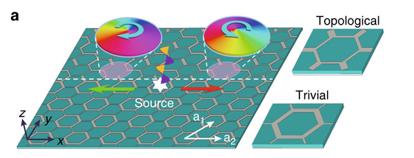
Figure: Microstrip system capable of hosting electromagnetic modes with orbital angular momentum.
Metamaterials are purposely built devices mimicking structural features of normal materials, but with unusual physical properties. Photonic crystals, for example, are periodic nanostructures consisting of material components with different refractive indices. They have lattice symmetries like solids, but the constituents of the unit cell of a photonic crystal are ‘bits’ of the different bulk materials. Similar to the structure–property relationships resulting from the behavior of electrons in solids (e.g. semiconduction), photonic crystals offer ways for manipulating the propagation of light. Now, Xiao Hu at the International Center for Materials Nanoarchitectonics, National Institute for Materials Science, Tsukuba, Japan, and colleagues have succeeded in creating a photonic metamaterial that displays a special property known as a topological photonic state.
The researchers first considered theoretically a planar construction of microstrips organized in a honeycomb-like way. Strip segments inside hexagons are put narrower than those between hexagons in one half of the device, and vice versa in the other half, because a structure with alternatingly wide and narrow strips results in a so-called photonic band gap: a range of frequencies for which electromagnetic waves cannot naturally exist in the system. The nodes of the hexagonal network are connected to capacitors; the segments linking nodes act as inductors. (A capacitor, abbreviated ‘C’ in circuit theory, is an electric component capable of storing energy in an electric field. An inductor, abbreviated ‘L’, is a component that stores energy in a magnetic field when an electric current flows through it.)
The topological LC-circuit proposed by Hu and colleagues has a peculiar property. When excited by an electromagnetic wave with a frequency in the photonic band gap, at the intersection of the two halves, waves in opposite directions are created. What is remarkable is that these two waves can be assigned a quantity known as pseudospin, with values ‘up’ and ‘down’, respectively, and they are immune to backscatter even at sharp corners and robust to defects due to the topological protection.
To demonstrate their theoretical finding experimentally, the scientists fabricated the topological LC circuit from microstrips — metallic strip lengths were about 1 cm and both halves consisted of 14 × 8 hexagons — and, by using microwave near-field techniques, measured the electric-field component perpendicular to the sample. The measurements confirmed the existence of the special topological state.
Being able to generate and manipulate electromagnetic waves with pseudospin is promising for applications like communications and high-resolution imaging. The concept presented by Hu and colleagues is not restricted to the microwave range, but also applicable to infrared light. The planar geometry of the device makes it easy to include other circuit elements, such as resonators or superconducting Josephson junctions. One difficulty, though, is to channel the pseudospin modes out of the sample. As the scientists point out: “[To] figure out a way to emit efficiently electromagnetic modes [with pseudospin] ... supported by the microstrip structure ... into free space is one of the most intriguing future problems.”
Reference
“Topological LC-circuits based on microstrips and observation of electromagnetic modes with orbital angular momentum”
Yuan Li, Yong Sun, Weiwei Zhu, Zhiwei Guo, Jun Jiang, Toshikaze Kariyado, Hong Chen, and Xiao Hu
Journal : Nat. Comms. 9, 4598 (2018).
DOI : 10.1038/s41467-018-07084-2
Yuan Li, Yong Sun, Weiwei Zhu, Zhiwei Guo, Jun Jiang, Toshikaze Kariyado, Hong Chen, and Xiao Hu
Journal : Nat. Comms. 9, 4598 (2018).
DOI : 10.1038/s41467-018-07084-2
Affiliations
International Center for Materials Nanoarchitectonics (WPI-MANA), National Institute for Materials Science (NIMS), Namiki 1-1, Tsukuba, Ibaraki 305-0044, Japan
Contact information
ナノアーキテクトニクス材料研究センター (MANA)
〒305-0044 茨城県つくば市並木1-1
TEL: 029-860-4710
E-mail: mana-pr=ml.nims.go.jp([ = ] → [ @ ] )
TEL: 029-860-4710
E-mail: mana-pr=ml.nims.go.jp([ = ] → [ @ ] )