- ホーム
- > 研究活動
- > Research Highlights
- > Vol. 40 Breakthrough in Printed Electr・・・
 Research Highlights
[Vol. 40]
Breakthrough in Printed Electronics Enables Device Formation at Room Temperature
- 前の記事
- 一覧に戻る
- 次の記事
2018.07.01
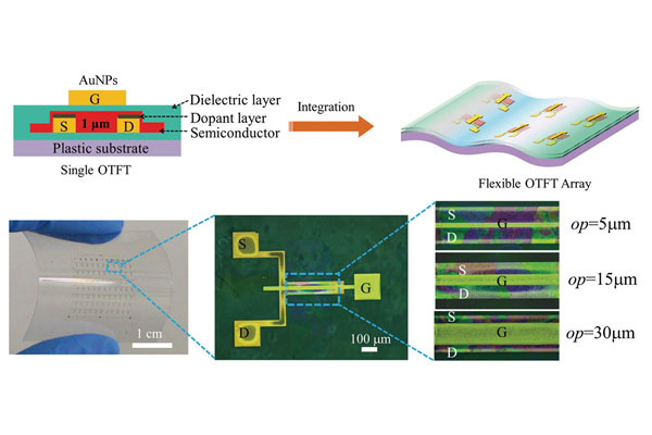
Figure: Multilayered structures of single OTFTs, and homogeneous integration of OTFT devices into large-scale OTFT array; and image of short-channel OTFTs spontaneously fabricated on the plastic substrate, photograph of a bottom-contact/top-gate OTFT.
Printing electronic devices and circuits on flexible substrates offers the possibility of low cost, mass production of high performance organic thin film devices using technology such as “roll-to-roll”.
However, conventional printing technology necessities processing at elevated temperatures of about 150°C, which damages flexible substrates causing degradation of device performance and limits the minimum feature sizes of devices.
The high temperature step is necessary to remove non-conductive ligands attached to metal nanoparticles (NP) used in the printing ink that is used for fabricating electrodes.
To resolve this issue Takeo Minari and colleagues at the World Premier International Center for Materials Nanoarchitectonics (WPI-MANA), National Institute for Materials Science (NIMS), Tsukuba, Japan have succeeded in printing organic field effect transistor (OFET) circuits on flexible substrates at room temperature. Importantly, the devices show remarkable performance as exemplified by the high average mobility of 8 cm2 V-1 s-1 of devices, that is necessary for practical applications.
Furthermore, Xuying Liu and colleagues fabricated large‐scale, complex electronic circuits with high resolution (1 μm). The prepared organic thin‐film transistors exhibit a low contact resistance of 1.5 kΩ cm, and high mobilities of 0.3 and 1.5 cm2 V−1 s−1 in the devices with channel lengths of 1 and 5 μm, respectively.
Kanehara, Minari and colleagues developed so called π-junction gold NPs (AuNPs) that are covered with phthalocyanine conductive ligands and do not require annealing to produce electrical conduction after ink printing.
Importantly, the electrical resistivity of AuNPs is approximately 9 × 10⁻⁶ Ω cm, which is almost the same as pure Au. This approach works without annealing because the charge is transported between nanoparticles via the conductive ligands.
“The importance of these results is that electronic circuit can be formed by simply applying ink at room temperature under normal atmospheric conditions,” says Minari. “This breakthrough means that circuits can be easily fabricated on the surfaces of materials that are sensitive to heat such as paper and plastics. Also, printed circuits can be produced with precision down to one micrometer, thereby making this a practical technology for real life applications.”
Reference
“Room-Temperature Printing of Organic Thin-Film Transistors with π -Junction Gold Nanoparticles”
Takeo Minari, Yuki Kanehara, Chuan Liu, Kenji Sakamoto, Takeshi Yasuda, Asuka Yaguchi, Shigemi Tsukada, Kei Kashizaki, and Masayuki Kanehara
Journal : Adv. Funct. Mater. 24, 4886–4892, (2014).
DOI : 10.1002/adfm.201400169
“Spontaneous Patterning of High-Resolution Electronics via Parallel Vacuum Ultraviolet”
Xuying Liu, Masayuki Kanehara, Chuan Liu, Kenji Sakamoto, Takeshi Yasuda, Jun Takeya, and Takeo Minari
Journal : Adv. Mater. 28, 6568–6573, (2016).
DOI : 10.1002/adma.201506151
Affiliations
International Center for Materials Nanoarchitectonics (WPI-MANA), National Institute for Materials Science (NIMS), Namiki 1-1, Tsukuba, Ibaraki 305-0044, Japan
Contact information
ナノアーキテクトニクス材料研究センター (MANA)
〒305-0044 茨城県つくば市並木1-1
TEL: 029-860-4710
E-mail: mana-pr=ml.nims.go.jp([ = ] → [ @ ] )
TEL: 029-860-4710
E-mail: mana-pr=ml.nims.go.jp([ = ] → [ @ ] )