- ホーム
- > 研究活動
- > Research Highlights
- > Vol. 30 Topological Photonic Crystal M・・・
 Research Highlights
[Vol. 30]
Topological Photonic Crystal Made of Silicon
- 前の記事
- 一覧に戻る
- 次の記事
2017.01.19
WPI-MANA researchers derive topological photonic states purely based on silicon, which can lead to the development of new functions and devices through integration with semiconductor electronics
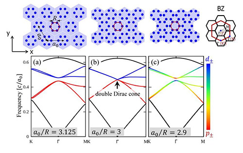
Figure: (Top) Schematic of photonic crystals consisting of nanorods derived from the honeycomb lattice viewed from above, and (bottom) the corresponding photonic bands. Photonic crystals are obtained by dividing the nearest neighboring nanorods into hexagonal clusters, and widening (a) or narrowing (c) the separation between the hexagonal clusters from the original honeycomb lattice (b), while maintaining the same shape and size of the hexagons. In (c), a band inversion occurs between the photonic p- and d-bands, which generates topological features in the system.
Topology is a mathematical concept which describes the way of connection of an object invariant under continuous deformation. Recently, it has been pointed out that topology can also be defined in the electronic states of materials, and this provides a unified and useful picture for physicists describing the unique properties of materials.
Based on a new approach which they have dubbed “topological nanoarchitectonics,” Xiao Hu and Long-Hua Wu, who are theoreticians at the International Center for Materials Nanoarchitectonics (MANA), National Institute for Materials Science (NIMS), elucidated a new principle which makes electromagnetic waves including light propagate on the edge in a two-dimensional photonic crystal without being scattered.
It was known that scattering of light by defects in conventional photonic crystals can be suppressed in topological photonic states, but so far special materials were required in order to create topological photonic crystals. However, the MANA researchers discovered a new principle which makes it possible to realize a topological photonic crystal by merely adjusting the positions of insulator or semiconductor nanorods in a honeycomb lattice, without using any special material or complicated structure. When hexagonal clusters are formed by adjusting the positions of nanorods, electromagnetic modes carrying spin, which is conventionally specific to electrons, appear. As a result, the MANA researchers theoretically clarified that a photonic crystal exhibits topological properties when the separation between hexagonal clusters is narrowed from that of the honeycomb lattice.
Since this new property of a photonic crystal can be obtained even by semiconductor such as silicon and/or GaN alone, various new functions are expected by integration of information processing functions achieved by the well-established semiconductor electronics and the excellent topological property of electromagnetic waves.
Reference
"Scheme for Achieving a Topological Photonic Crystal by Using Dielectric Material"
Long-Hua Wu and Xiao Hu
Journal : Phys. Rev. Lett. 114 (2015) 223901.
DOI : 10.1103/PhysRevLett.114.223901
Long-Hua Wu and Xiao Hu
Journal : Phys. Rev. Lett. 114 (2015) 223901.
DOI : 10.1103/PhysRevLett.114.223901
Affiliations
International Center for Materials Nanoarchitectonics (WPI-MANA), National Institute for Materials Science (NIMS), Namiki 1-1, Tsukuba, Ibaraki 305-0044, Japan
Contact information
ナノアーキテクトニクス材料研究センター(MANA)
〒305-0044 茨城県つくば市並木1-1
TEL: 029-860-4710
E-mail: mana-pr=ml.nims.go.jp([ = ] → [ @ ] )
TEL: 029-860-4710
E-mail: mana-pr=ml.nims.go.jp([ = ] → [ @ ] )