- ホーム
- > 研究活動
- > Research Highlights
- > Vol. 19 Visualizing superconductive c・・・
 Research Highlights
[Vol. 19]
Visualizing superconductive coupling over atomic steps
- 前の記事
- 一覧に戻る
- 次の記事
2015.02.27
Scanning tunnelling microscopy imaging under differing magnetic fields gives fundamental insights into the behavior of supercurrents and vortices on the surface of indium-doped silicon films.
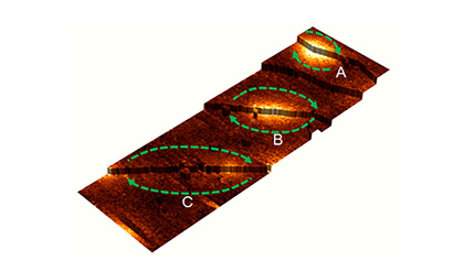
Figure : Scientists at the International Center for Materials Nanoarchitectonics have uncovered how supercurrents flow over atomic steps and terraces on indium-covered silicon surface. Vortices trapped at the atomic steps change their characters from Pearl to Josephson vortices (from A to C). These reflect change in strength of Josephson coupling between the neighboring terraces.
Superconductors have effectively zero resistance and act as perpetual carriers of electric current with no need for a connected power source. As such they have many applications in electronics. One of the thinnest two-dimensional materials ever created, called Si(111)-(√7 x √3)-In –individual indium metal atoms added to a silicon surface - recently surprised scientists with its superconducting abilities. The race is now on to find out how and why this silicon surface is capable of superconductivity, as well as what uses it may have.
Takashi Uchihashi and co-workers at the International Center for Materials Nanoarchitectonics, Tsukuba, together with scientists across Japan, have now uncovered the underlying structures and the behavior of currents on the surface of Si(111)-(√7 x √3)-In which provide clues to its superconductivity.
The silicon surface comprises individual terraces separated by steps measuring the height of a single atom (‘atomic steps’). These steps could potentially interrupt, or decouple, neighboring terraces and break the current flowing over large surfaces. Uchihashi and his team used a scanning tunnelling microscope in order to verify how superconductivity occurs in the presence of atomic steps and terraces. The team applied different magnetic fields, which influenced the strength of the current and the presence of associated vortices.
By taking a series of images of the silicon, the team uncovered a pattern of supercurrent vortices present on the silicon surface. Two vortex types were present. Pearl vortices were present on the terrace surfaces, and appeared as bright round features in the images. However, at the atomic steps the vortices appeared to become trapped and altered in character. These elongated ‘Josephson vortices’ give evidence that the atomic steps work as so-called Josephson junctions, allowing coupling to occur across stepped terraces and enabling supercurrents to flow. The idea was firmly established with the help of microscopic theoretical calculations.
Reference
"Imaging Josephson vortices on the surface superconductor using a scanning tunnelling microscope"
Shunsuke Yoshizawa, Howon Kim, Takuto Kawakami, Yuki Nagai, Tomonobu Nakayama, Xiao Hu, Yukio Hasegawa, and Takashi Uchihashi
Journal : Physical Review Letters (highlighted as an Editors' Suggestion) (2014).
DOI : 10.1103/PhysRevLett.113.247004
Shunsuke Yoshizawa, Howon Kim, Takuto Kawakami, Yuki Nagai, Tomonobu Nakayama, Xiao Hu, Yukio Hasegawa, and Takashi Uchihashi
Journal : Physical Review Letters (highlighted as an Editors' Suggestion) (2014).
DOI : 10.1103/PhysRevLett.113.247004
Affiliations
International Center for Materials Nanoarchitectonics (WPI-MANA), National Institute for Materials Science (NIMS), Namiki 1-1, Tsukuba, Ibaraki 305-0044, Japan
Contact information
ナノアーキテクトニクス材料研究センター(MANA)
〒305-0044 茨城県つくば市並木1-1
TEL: 029-860-4710
E-mail: mana-pr=ml.nims.go.jp([ = ] → [ @ ] )
TEL: 029-860-4710
E-mail: mana-pr=ml.nims.go.jp([ = ] → [ @ ] )