- ホーム
- > 研究活動
- > Research Highlights
- > Vol. 16 A cool approach to flexible el・・・
 Research Highlights
[Vol. 16]
A cool approach to flexible electronics
- 前の記事
- 一覧に戻る
- 次の記事
2014.07.10
A nanoparticle ink that can be used for printing electronics without high-temperature annealing presents a possible profitable approach for manufacturing flexible electronics.
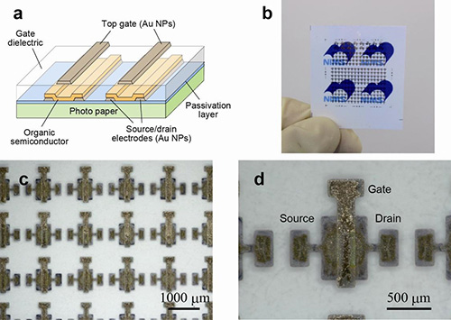
Figure : Fully printed organic thin film transistors (OTFTs) on a paper substrate. (a) Schematic of the device structure for a fully printed OTFT on paper. (b) Arrays of fully printed OTFTs fabricated on a paper substrate inkjet printed with the NIMS logo before adding the device. (c) An optical microscope image of fully-printed OTFT arrays. (d) A magnified optical microscope image of the individual device. Arrays of fully printed organic thin film transistors fabricated on paper substrates that had the the NIMS logo ink jet printed on before processing.
Printing semiconductor devices is considered to provide low-cost high performance flexible electronics that outperforms the amorphous silicon thin film transistors currently limiting developments in display technology. However the nanoparticle inks developed so far have required annealing, which limits them to substrates that can withstand high temperatures, ruling out a lot of the flexible plastics that could otherwise be used. Researchers at the National Institute for Materials Science and Okayama University in Japan have now developed a nanoparticle ink that can be used with room-temperature printing procedures.
Developments in thin film transistors made from amorphous silicon have provided wider, thinner displays with higher resolution and lower energy consumption. However further progress in this field is now limited by the low response to applied electric fields, that is, the low field-effect mobility. Oxide semiconductors such as InGaZnO (IGZO) offer better performance characteristics but require complicated fabrication procedures.
Nanoparticle inks should allow simple low-cost manufacture but the nanoparticles usually used are surrounded in non-conductive ligands – molecules that are introduced during synthesis for stabilizing the particles. These ligands must be removed by annealing to make the ink conducting. Takeo Minari, Masayuki Kanehara and colleagues found a way around this difficulty by developing nanoparticles surrounded by planar aromatic molecules that allow charge transfer.
The gold nanoparticles had a resistivity of around 9 x 10⁻⁶ Ω cm – similar to pure gold. The researchers used the nanoparticle ink to print organic thin film transistors on a flexible polymer and a paper substrate at room temperature, producing devices with mobilities of 7.9 and 2.5 cm2 V-1 s-1 for polymer and paper respectively – figures comparable to IGZO devices.
Reference
"Room-temperature printing of organic thin-film transistors with π-junction gold nanoparticles"
Takeo Minari, Yuki Kanehara, Chuan Liu, Kenji Sakamoto, Takeshi Yasuda, Asuka Yaguchi, Shigemi Tsukada, Kei Kashizaki, Masayuki Kanehara
Journal : Advanced Functional Materials 24, 31, 4886-4892 (2014).
DOI : 10.1002/adfm.201400169
Takeo Minari, Yuki Kanehara, Chuan Liu, Kenji Sakamoto, Takeshi Yasuda, Asuka Yaguchi, Shigemi Tsukada, Kei Kashizaki, Masayuki Kanehara
Journal : Advanced Functional Materials 24, 31, 4886-4892 (2014).
DOI : 10.1002/adfm.201400169
Affiliations
International Center for Materials Nanoarchitectonics (WPI-MANA), National Institute for Materials Science (NIMS), Namiki 1-1, Tsukuba, Ibaraki 305-0044, Japan
Contact information
ナノアーキテクトニクス材料研究センター(MANA)
〒305-0044 茨城県つくば市並木1-1
TEL: 029-860-4710
E-mail: mana-pr=ml.nims.go.jp([ = ] → [ @ ] )
TEL: 029-860-4710
E-mail: mana-pr=ml.nims.go.jp([ = ] → [ @ ] )