MANA International Symposium 2025
Semiconductor Materials - 12
Title
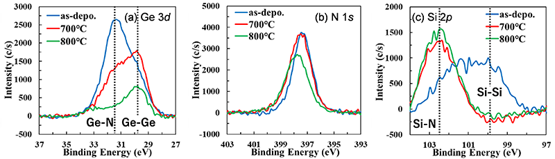
Germanium nanosheet formation by selective nitrogen removal from amorphous GeN films

Authors
Affiliations
Semiconductor Device Group, MANA, NIMS
URL
https://www.nims.go.jp/group/semidev/
HOSOI.Takuji@nims.go.jp
Abstract
To advance transistor scaling in integrated circuits, semiconductor nanosheets with high crystallinity and surface flatness are essential. Theoretical study on electron mobility for 2 nm-thick nanosheets suggested that Ge(111) nanosheets may offer an order of magnitude higher than Si nanosheets
This study explores a novel method based on prior work
Reference
- K. Sumita et al., IEEE Trans. Electron Devices 69, 2115 (2022). DOI: 10.1109/TED.2022.3143484
- K. Kutsuki et al., Jpn. J. Appl. Phys. 47, 2415 (2008). DOI: 10.1143/JJAP.47.2415