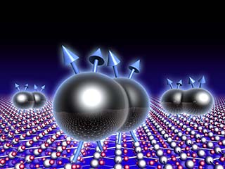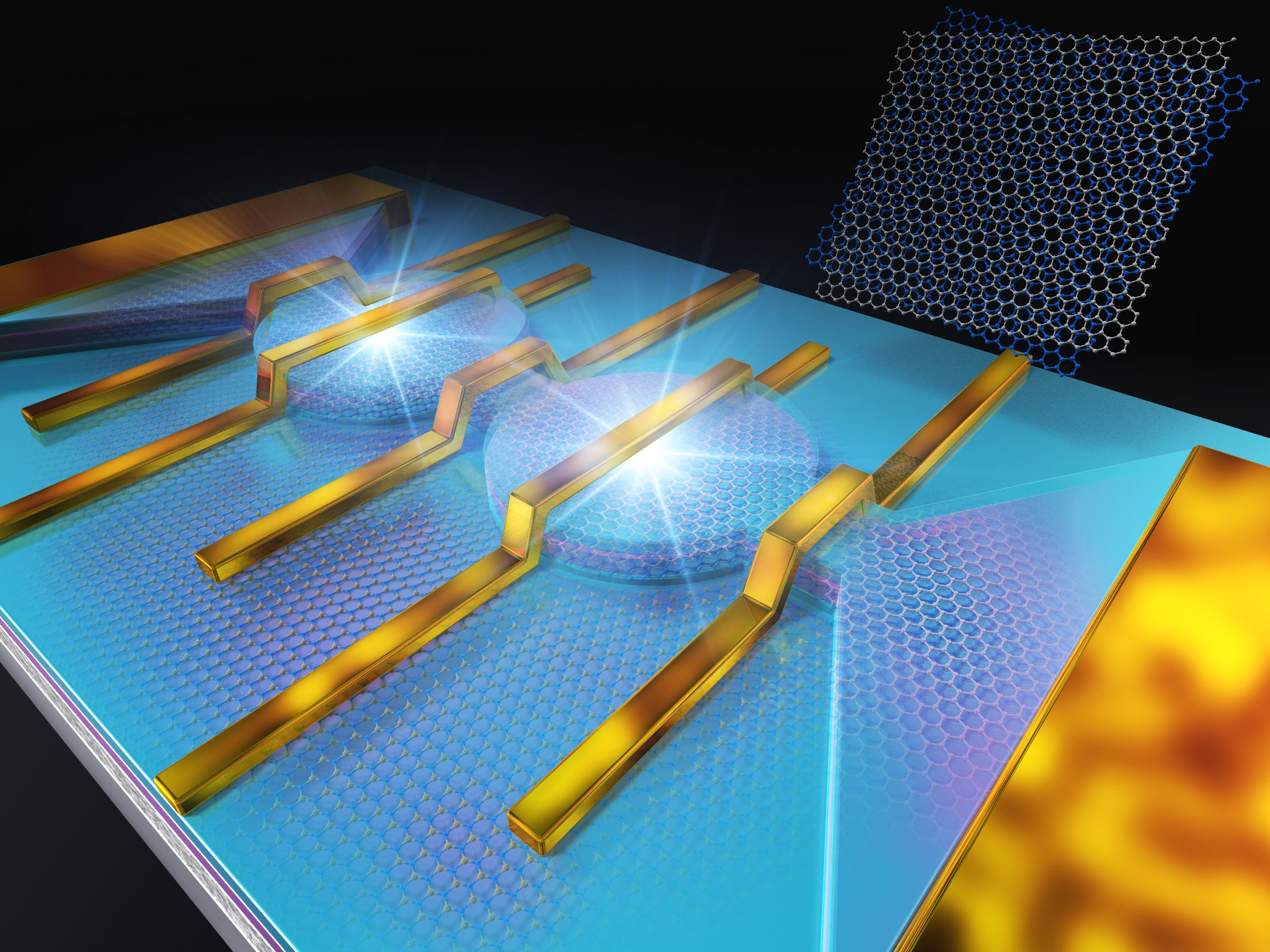
電子のスピンやバレーを量子ビットの媒体として用いるための半導体材料の開発を行っています。半導体量子ビットは近接電子間の交換相互作用を用いるので、100nm程度の間隔で並べられ、集積化に優れています。本研究では、従来半導体量子ビットの研究で用いられてきたGaAsやSiに替わり、電子の量子コヒーレンスのさらなる向上や制御手法の 多様化が可能となる新たな材料の開拓を行っています。材料の作製から、微細加工プロセスの開発、特性評価までグループ内外の協力の元進めています。
We are developing semiconductor materials to place electron spins and valleys as media for quantum bits. In this research, we are searching for new materials that will enable further progress in quantum coherence of electrons and diversification of control methods, in place of GaAs and Si, which have been used in conventional semiconductor qubit research. We are collaborating both within and outside the group, from fabrication to microfabrication We investigate semiconductor materials for qubits utilizing electron spin or valley degree of freedom. We aim for new materials that enable further progress in quantum coherence and enhance the control and detecting schemes, compared with GaAs and Si, which have been used in conventional semiconductor qubit research. We are collaborating both within and outside the group, from material synthesis and microfabrication to low-temperature evaluation.process development and property evaluation.
Articles- "Parity-independent Kondo effect of correlated electrons in electrostatically defined ZnO quantum dots"
Nature Communications 15, 9556 (2024) - "Single-carrier transport in graphene/hBN superlattices"
Nano Letters 20, 2551-2557 (2020) - "Quantized conductance of one-dimensional strongly correlated electrons in an oxide heterostructure"
Physical Review B 99, 121302(R)-1-6 (2019)