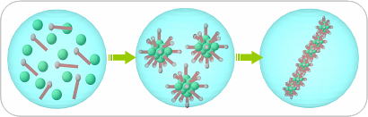
The Fine Particle Processing Group focuses on the synthesis and characterization of nanoparticles,
assembling of nanoparticles and the fabrication of novel ceramics with unique microstructure
and complex material combination in a variety of morphologies and dimensions.
We also address the design of hetero interfaces formed on inorganic materials and the construction of
devices for electrical applications.
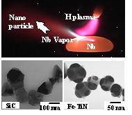
| Synthesis of nano particles by using reactive thermal plasmas | |
|
Schematic illustration for reactive thermal plasma processing forming inorganic nanoparticles, (left below) SiC nanoparticle prepared by nitrogen plasma, and (right below) Fe-TiN nano-composite particle prepared by a mixture of hydrogen and nitrogen plasmas. |
| Control over Heterogeneous Nanointerface of Realizing a Mass Transfer | |
 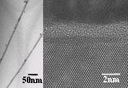 |
(Left) STEM image of a free-standing fibril-like nanostructure of silicon, (Right) Cross-sectional HR-TEM image of organic monolayer covalently attached to silicon surface. Since the monolayer is directly immobilized onto bare silicon, a mass transfer is achieved through the hetero-interface. |
| Fabrication of self-organized photonic crystals for laser applications | |
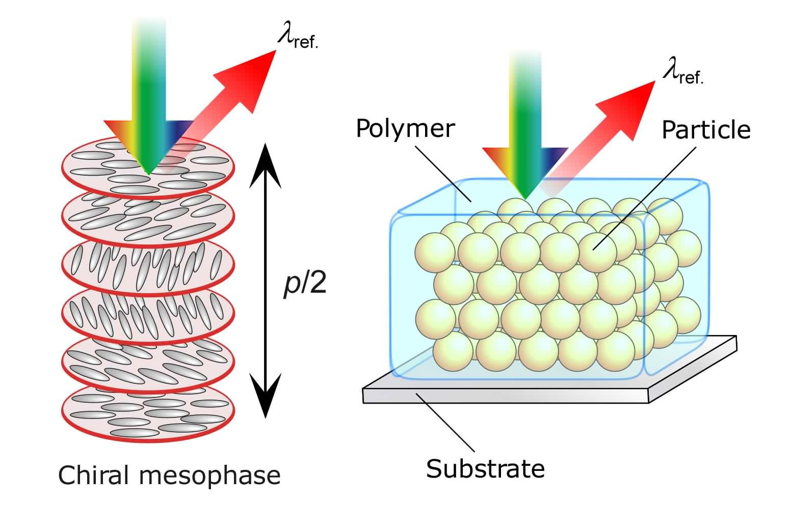 |
Self-organized photonic crystals structures used in this study. (Left) Supramolecular helical structures of chiral molecules at the liquid crystal phase. (Right) 3-D ordered structure of submicrometer polymer particles on substrate. |
| Electrochemical techniques for shaping novel ceramics | |
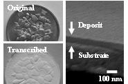 |
(Left) Alumina free-standing film with a complicated pattern of a coin fabricated by electrophoretic deposition (EPD). (Right) Anatase thin film deposited on Si substrate prepared by electrolytic deposition (ELD). |
| Utilization of high magnetic field for innovative materials processing | |
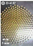 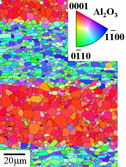 |
(Left) Self-organization of gold spheres due to the magnetically induced dipoles interaction. (Right) EBSD map of alumina/alumina laminar composites with different crystalline-oriented layers produced by EPD in the magnetic field of 12 T. |