Simultaneous Measurement of Electronic Properties and Optical Properties of Organic EL Realized in the Atmosphere
Accelerates Development of New Materials for Organic EL by Fast and Simple Measurement Device
2012.08.27
(2012.10.09 Update)
National Institute for Materials Science
A research group at the NIMS International Center for Materials Nanoarchitectonics (MANA) succeeded in the development of band diagram measurement system in atmospheric condition for organic semiconductor materials such as organic light emitting device (OLED). This equipment enables simple, high speed measurement of the band diagrams of organic semiconductor materials in the atmosphere. Band diagram shows absolute value of higher occupied molecular orbital (HOMO) energy level and lower unoccupied molecular orbital (LUMO) energy level based on the vacuum level. The developed system is a combination of a spectrophotometer system and a photoemission yield system in atmospheric condition. We can be obtained the optical property (Band gap) and the electric property (Ionized potential) at the same time. This system can be applied to the development of a variety of materials and devices.
Abstract
- A research group including Dr. Toyohiro Chikyo, Unit Director of the Semiconductor Device Materials Group of the Nano-electronic Materials Unit, International Center for Materials Nanoarchitectonics (MANA; Director-General: Masakazu Aono), National Institute for Materials Science (President: Sukekatsu Ushioda), and Dr. Shinjiro Yagyu, MANA Scientist, Dr. Michiko Yoshitake, MANA Scientist, Dr. Masahiro Goto, MANA Principal Scientist, all of the same group, succeeded in developing a equipment that enables simple, high speed measurement of the band diagrams of organic semiconductor materials in the atmosphere.
- High expectations are placed on organic EL devices as next-generation lighting devices that will replace conventional incandescent light bulbs and fluorescent lights. Organic EL devices consist of a layered structure of an organic semiconductor with light-emitting, electron/hole transport properties, etc. enclosed between electrodes, and emit light when an electric current is passed. The properties and mass production of organic EL devices is largely controlled by the organic semiconductor materials, and in their development, it is important to know the band diagram, which includes information on both electronic properties and optical properties. However, until now, it was not possible to obtain band diagrams without using two or more measuring system. This resulted in various problems, such as the method of setting the measurement specimens, degradation of materials due to differences in the measurement environment (e.g., vacuum and other environments), and excessive measurement time, among others.
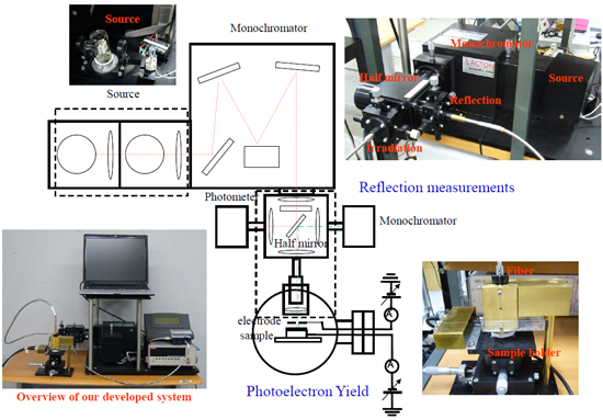
- The team headed by Dr. Yagyu developed a equipment which enables measurement of both the electronic properties and the optical properties necessary in band diagrams simultaneously and in the atmosphere. Measurements are performed by irradiating light from the ultraviolet region to the near-infrared region on the specimen, and simultaneously measuring the light which is reflected or transmitted, and the electrons which are emitted as a result of the photoelectric effect. Accurate band diagrams can be obtained rapidly using this method. In atmospheric measurement, electrons collide with oxygen and nitrogen in the air, preventing scattering to a distance. As a result, with the newly-developed equipment, simultaneous measurement is possible by positioning the electrodes used to collect electrons in close proximity to the specimen not to interfere with reflection measurements.
- In this research, high speed and high accuracy were realized in measurements, as it is only necessary to set the specimen in the measurement device once, and information on both the electronic properties and the optical properties necessary in the band diagram can be obtained simultaneously. This results in a smooth flow from material development to measurement, and thus can accelerate new material development.
- This research result had been announced at the 73rd Japan Society of Applied Physics (JSAP) Autumn Meeting held September 11-14, 2012 in Matsuyama City, Ehime Prefecture.

Figure: Outline of the developed atmospheric organic semiconductor band diagram measurement equipment.