1. Introduction
In terms of the research of recent advanced materials or nano-materials, microstructure analysis becomes important and it requires ultra high spatial resolution. Electron energy-loss spectroscopy in transmission electron microscopy (TEM-EELS) and energy-filtering TEM (EFTEM) are powerful tools to analyze the microstructure. Elemental and chemical (bonding) maps can be observed using EFTEM. In this presentation, we will show a few applications of EFTEM and recent developments/improvements in TEM-EELS.
2. Applications of high-resolution elemental/chemical mapping
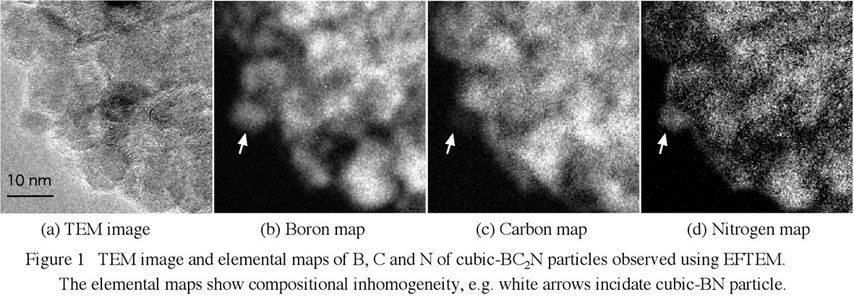
a. Elemental mapping of cubic-BCN fine particles
Figure 1 shows the TEM image and the elemental maps of cubic BC2N fine particles. The bright contrast of the elemental maps indicates the existence of each element. The specimen was synthesized under 18 GPa at 1500űC. The specimen is polycrystalline and consists of fine particles about 10 nm in diameter. The elemental maps show compositional inhomogeneity. The B and N maps show the same contrast, but are different from the C map. This shows the initial state of a phase separation into cubic-BN and diamond. Since the grain size of the present specimen is small, this phase separation is difficult to detect using X-ray diffraction.
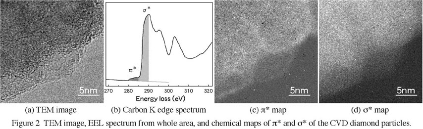
b. Chemical mapping of CVD diamond particles
We observe the microstructure of diamond particles formed by low pressure inductively coupled plasma CVD (chemical vapor deposition) [1]. Figure 2a shows the TEM image of the diamond particles. The diameter of diamond particle is few hundred nm, but the particle consists of smaller sub-grains of approximately 20-50 nm in diameter. The EEL spectrum of a whole area (Fig. 2b) shows not only s* but also p* peak which is originated from sp2 bonding. We observe 4 energy-filtered images with a narrow energy window of 5 eV, and extract p* and s* maps (Figs. 2c and 2d). It is found that the grain boundaries and the surface of the sub-grain have sp2 bonding. The bonding maps obtained will give us useful information in controlling the grain size of nanocrystalline diamond particles and in optimizing the growth conditions in the CVD process.
3. Improvements of TEM-EELS and EFTEM techniques.
For research and development of nano-materials, TEM and EELS techniques should also be improved. The following techniques were developed during this COE project, and were applied for recent microanalyses: (i) Practical coma-free alignment method for high-resolution TEM [2]. (ii) High-sensitivity EELS analysis by detector-gain correction [3]. (iii) Spatially-resolved EELS technique using EFTEM [4]. (iv) Ab initio calculation for the interpretation of energy-loss near edge structure (ELNES) [3,5]. (v) Software techniques for 0.3 eV energy resolution [6].
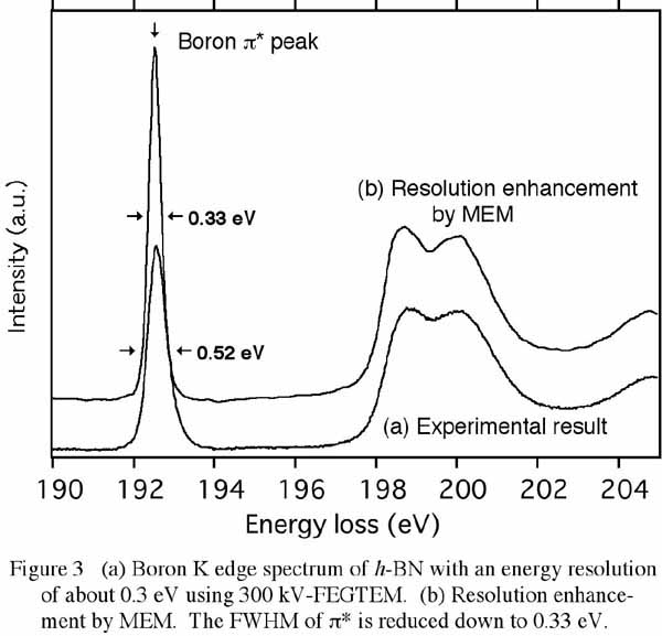
Figure 3 shows one demonstration of the technique (v) for the core-loss spectrum of h-BN. The spectrum was obtained using 300 kV-FEGTEM (Hitachi, HF-3000) with energy filter (Gatan, GIF2002). Boron-K edge p* peak shows a narrow energy spread of 0.52 eV in FWHM (full-width at half maximum). Recently we have applied a resolution-enhancement technique based on maximum entropy method [7], and the p* FWHM is reduced down to 0.33 eV, which is almost equal to that obtained using monochromator [8,9]. Using these techniques we can reach the ultimate energy-resolution, which is limited by life-time broadening.