1989-1994: Asahi Glass Company, Research Center in Yokohama
1991-1992: ERATO Kunitake Molecular Architecture project in Kurume
1994-1999: Postdoctoral position in ERATO Tanaka
Solid Junction Project in Yokohama and Max-Planck Institute for
Microstructure Physics in Halle, Germany
1999-present: Senior researcher in the Advanced Electronic
Material Center at the National Institute for Materials Science
【Research interest】
Original background is semiconductor materials science, including nanostructure fabrication,
thin film growth and their characterization.
Recently, his interest moved molecular electronics: single-molecular electronics,
molecular self-assembly, thin film transistor and so on.
1. Molecular Coulomb islands for single-electron devices
Contribution of the metel/SiO2 interface potential to photo-induced switching in molecular
single-electron tunneling junction
Y. Noguchi, T. Kubota, S. Mashiko, Y. Wakayama
Journal of Applied Physics 97 (2005) 073513.
Optical switching of single-electron tunneling in SiO2/molecule/SiO2 multilayer on Si(100)
Y. Wakayama, K. Ogawa, T. Kubota, H. Suzuki, T. Kamikado and S. Mashiko
Appl. Phys. Lett. 85 (2004) 329
Optical controllability of single-electron tunneling through molecular Coulomb island in MOS structure
Y. Wakayama, T. Kubota, H. Suzuki, T. Kamikado and S. Mashiko
Nanotechnology 15 (2004) 1446-1449.
Molecular Coulomb islands for single-electron tunneling in SiO2/molecules/SiO2
multilayers on Si(100)
Y. Wakayama, T. Kubota, H. Suzuki, T. Kamikado and S. Mashiko
J. Applied Physics 94 (2003) 4711
Assembly process and epitaxy of the F16CuPc monolayer on Cu(111)
Yutaka Wakayama
Journal of Physical Chemistry C 111 (2007) 2675-2678.
2D Supramolecular Assembling as a function of the concentration and substrate: a catalogue of Binary Monolayers
E. Barrena, Dimas G. de Oteyza, H. Dosch, Y. Wakayama
ChemPhysChem 8 (2007) 1915-1918.
Self-Assembly Structures of a Phenol-Substituted Porphyrin in the Solid State: Hydrogen Bonding,
Kagom & eacute; Lattice and Defect Tolerance
Jonathan P. Hill, Yutaka Wakayama, Misaho Akada, Katsuhiko Ariga
Journal of Physical Chemistry C 111 (2007) 16174-16180.
Real-time STM observation of molecular dynamics on a metal surface
Yutaka Wakayama, Jonathan P. Hill and Katsuhiko Ariga
Surface Science 601 (2007) 3984-3987.
Crystallographic and electronic structure of self-assembled DIP monolayers on Au(111) substrates
Dimas G. de Oteyza, Esther Barrena, Miguel Ruiz-Osés, Iñaki Silanes, Bryan P. Doyle,
J. Enrique Ortega, Andrés Arnau, Helmut Dosch, Yutaka Wakayama.
Journal of Physical Chemistry C 112 (2008) 7168-7172.
Balancing intermolecular and molecule-substrate interactions in supramolecular assemblies.
Dimas G. de Oteyza, Iñaki Silanes, Miguel Ruiz-Osés, Esther Barrena, Bryan P. Doyle, Andrés Arnau,
Helmut Dosch, Yutaka Wakayama and J. Enrique Ortega
Advanced Functional Materials 19 (2009) 259-264.
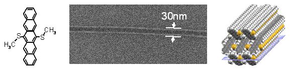
Self-assembled molecular nanowires of 6,13-bis(methylthio)pentacene: growth, electrical properties and applications
Yutaka Wakayama, Ryoma Hayakawa, Toyohiro Chikyow, Shinichi Machida, Tomonobu Nakayama, Stefan Egger,
Dimas G. de Oteyza, Helmut Dosch and Kenji Kobayashi
Nano Letters 8 (2008) 3273-3277.
Control of molecular packing structure of a derivative of vanadyl-phthalocyanine using pore wall of porous
alumina and/or magnetic field
Seiichi Takami, Yasuhiro Shirai, Yutaka Wakayama and Toyohiro Chikyow
Thin Solid Films 516 (2008) 2438-2442.
Synthesis of Octabutoxyphthalocyanine Nanorods Using Porous Alumina as a Template and Magnetic-Field
Directed Control of the Molecular Orientation in the Nanorods
Seiichi Takami, Yasuhiro Shirai, Yutaka Wakayama and Toyohiro Chikyow
Journal of Materials Chemistry 18 (2008) 4347-4350.
Light propagation through colloidal crystal wire fabricated by dewetting process
T. Mitsui, Y. Wakayama, T. Onodera, Y. Takaya, H. Oikawa
Nano Letters 8 (2008) 853-858.
4. Oganic thin film: growth mechanism and application
Stress Release Drives Growth Transition of Quaterrylene Thin Films on SiO2 Surfaces
Ryoma Hayakawa, XueNa Zhang, Matthieu Petit, Helmut Dosch, Toyohiro Chikyow, Yutaka Wakayama
Journal of Physical Chemistry C 113 (2009) 2197–2199.
Interface Engineering for Molecular Alignment and Device Performance of Quaterrylene Thin Films
Ryoma Hayakawa, Matthieu Petit, Toyohiro Chikyow, Yutaka Wakayama
Appl. Phys. Lett. 93 (2008) 153301-153303
Analysis of Carrier Transport in Quaterrylene Thin Film Transistors Formed Using Ultra-Slow Vacuum Deposition
Ryoma Hayakawa, Matthieu Petit, Yutaka Wakayama and Toyohiro Chikyow
Journal of Applied Physics 104 (2008) 0245061-0245065.
Evolution of Quaterrylene Thin Films on a Silicon Dioxide Surface Using an Ultra-Slow Deposition Technique
Ryoma Hayakawa, Matthieu Petit, Yutaka Wakayama and Toyohiro Chikyow
Journal of Physical Chemistry C 111 (2007) 18703-18707
Growth of quaterrylene thin films on a silicon dioxide surface using vacuum deposition
Ryoma Hayakawa, Matthieu Petit, Yutaka Wakayama and Toyohiro Chikyow
Organic Electronics 8 (2007) 631–634
Early stage of a perylene diimide derivative thin film growth on various Si(001) substrates
Matthieu Petit, Ryoma Hayakawa, Yutaka Wakayama, and Toyohiro Chikyow
Journal of Physical Chemistry C 111 (2007) 12747-12751.
Growth of anthracene derivative thin film with π-stacking structure
Hiroyuki Sasaki, Yutaka Wakayama, Toyohiro Chikyow, Esther Barrena, Helmut Dosch and Kenji Kobayashi
Appl. Phys. Lett. 88 (2006) 081907-081909.