|
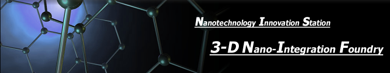
Multipurpose dry etching system (CCP-RIE) |
| |
|
Product |
RIE-200NL |
Manufacturer |
SAMCO International Inc. |
Capabilities |
RF frequency electric field with parallel plate
Process gasses: O2, SF6, CF4, CHF3, N2, Ar
Maximum wafer size: 6" wafer
Substrate temperature: RT ~ 30 degrees C |
|
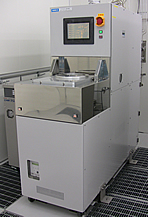
【Applications】 |
|
|
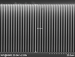
SiO2 etching with resist mask |
|
|
|
|
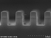
Compounds dry etching system (ICP–RIE) |
| |
|
Product |
RIE-100iPH |
Manufacturer |
SAMCO International Inc. |
Capabilities |
Inductively coupled plasma ( ICP ) induced type
Process gasses: O2、SF6、Ar、Cl2、BCl3、SiCl4、Xe
Maximum wafer size: 3" wafer
Substrate temperature: 50 ~ 200 degrees C |
|
【Applications】 |
|
|
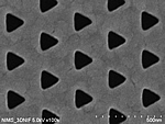
Triangular lattice pattern etching of
Aluminum thin film |
Si etching with SiO2 mask |
|
|
|
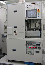
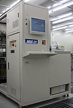
Dry etching system for oxide materials (operated by LCnet Project) |
| |
|
Product |
MUC-21 RV-APS-SE |
Manufacturer |
Sumitomo Precision Products Co. Ltd. |
Capabilities |
1. It is possible to perform high-rate and deep dry etching by high-density plasma optimized for oxides and compounds.
2. Various materials can be etched by eight different reactive gases.
3. All processes are automatic operations by PC control.
4. it can be carried out from basic research to production-type research since this system is adapted from small-piece samples to 6 inch wafers. |
|
【Applications】 |
|
|
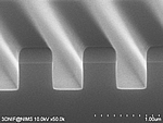
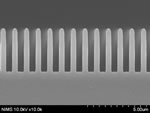
Fast and deep etching of SiO2
(Etching rate>0.5um/min) |
High aspect etching of SiO2
(Aspect ratio>10) |
|
|
|
Silicon deep etching system |
| |
|
Product |
MUC-21 ARE-SRE |
Manufacturer |
Sumitomo Precision Products Co. Ltd. |
Capabilities |
Inductively coupled plasma ( ICP ) induced type
Process gasses: SF6, C4F8, Ar, O2
Substrate size: 3" wafer (Maximum: 8" wafer)
Substrate Temperature: 5 ~ 35 degrees C
|
|
【Applications】 |
|
|
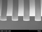
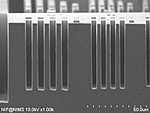
Silicon rectangular pattern etching |
Silicon line pattern etching
(depth 40um) |
|
|
|