|
Group Leader’s Greeting |
 |
 Group Leader
Yasuo Koide |
A mission of the Nano-Fabrication and Characterization Facility (NFCF) of the Interdisciplinary laboratory for Nanoscale Science and Technology (INST) is to create the innovation by providing advanced nanotechnology and micro-fabrication facilities and technical assistance for academia, industry, and government researchers.
The NFCF was launched at NIMS in FY2007 and had a 450-m2 clean room facility consisted of seven
rooms for each process; the process characterization, the film-deposition, the dry-etching, the thermalannealing,
the exposure & development, the photolithography, and the electron & laser beam lithography
areas. |
This facility has the advanced nano-scale observation, measurement, and characterization
systems and gives supports of three-dimensional fabrication with nanometer-to-millimeter scale for a variety of materials, such as semiconductor, oxide, dielectric, magnetic, and metallurgy, and composite materials with the aid of professional staffs.
Furthermore, the NFCF extensively promotes an interdisciplinary fusion research between natural and life sciences and collaboration among academia, industry, and government institute. Mutual exchanges among academia, industry, and government researchers in different fields will lead new perspective and unexpected discovery and innovation. |
|
|
|
|
Outline of Facilities |
|
|
|
|
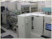
▲Thin film deposition area (Class1000) |
|
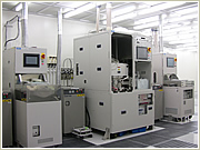
▲Dry etching area (Class1000) |
|
|
|
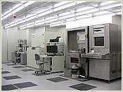
▲Process characterization area (Class1000) |
|
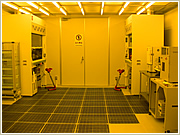
▲Yellow room(Class100) |
|
Facilities |
・ |
Clean room (450m2) and non-clean room laboratory |
・ |
Clean room facility consists of seven rooms for each process. |
| |
– Class 100(110m2): Electron beam & laser lithography, Photolithography, and Resist processing areas
– Class 1000(200m2): Film deposition, Thermal annealing, and Dry etching areas
– Class 10000(80m2): Process characterization area |
・ |
Non-clean room laboratory is for device characterization, cutting, and polishing process. |
| |
|
Materials |
・ |
Compound Semiconductors, Silicon, Oxide, Magnetic, Metal materials |
| |
|
Functions |
・ |
Photonic Crystals, Nano photonics, Nano carbons etc. |
| |
|
Main equipments |
・ |
Electron beam & laser lithography, ICP-RIE, Bosch, W-beam FIB etc. |
|
|
| |
|
|
Members |
|
Group Leader |
Yasuo KOIDE, Dr. |
 |
Senior Researcher |
Yoshimasa SUGIMOTO, Dr. |
|
Senior Engineer |
Naoki IKEDA, Dr. |
|
Senior Engineer |
Daiju TSUYA, Dr. |
|
Post Doctoral & Technical Staff |
NIMS Postdoctoral Researcher |
EiichiroWATANABE, Dr. |
|
NIMS Adjunct Researcher |
Kiyomi NAKAJIMA |
|
Contract Technical Staff |
Masayuki OCHIAI |
|
Contract Technical Staff |
Hirotaka OOSATO |
|
Contract Technical Staff |
|
|
Contract Technical Staff |
Etsuko URISAKA |
|
Contract Technical Staff |
Shushi HAMADA |
|
Contract Technical Staff |
Shuntaro TANIGAWA |
|
|
|
|
|