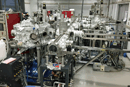
Thin Film Processing Instruments;
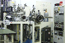
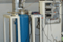
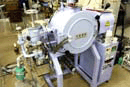
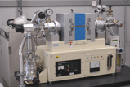
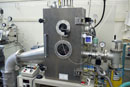
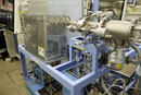
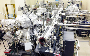 Ultra High Vauum Cluster-type
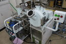
Sputtering Deposition System
UHV sputtering deposition system which has two sputtering chambers connected by the transfer chamber. Maximum 18 source can be deposited without air exposure in this system. High quality giant magnetoresistive device made by this system successfully realized the highest record of magnetoresistive property in the world.
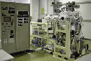
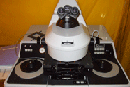
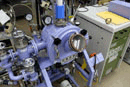
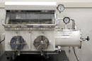
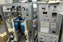
7 Targets UHV Co-Sputtering Machine
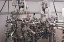
6 Targets UHV Rotating-Substrate Sputtering Machine
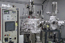
5 Targets UHV Sputtering Machine
5 Targets Magnetron Sputtering Machine
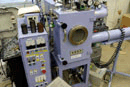
10 Targets UHV Sputtering Machine
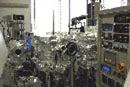
10 Targets Magnetron Sputtering Machine
Microfabrication Equipments;
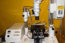
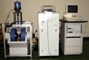
 JEOL Electron Beam Lithography JBX-6300SM
The electron beam lithography, which focus the highly accelerated electron and draw nano-scale pattern on resists, is an indispensable tool for testing new spintronics materials in actual device scale. Our equipment, JBX-6300 SM, can easily draw wire patterns down to 7 nm in width, due to the benefit of the highly acceleration voltage upto 100 kV. Fine correction functions enables semi-automatic exposure with high accuracy.
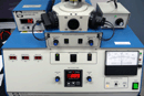
Mask Aligner
Mask Aligner
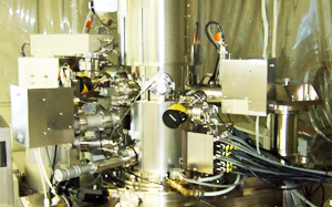
Ar Ion Milling Machine
S/TEM and TEM Specimen Prep. Equipments;
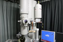
 FEI Titan G2 80-200
Titan G2 80-200 S/TEM(FEI) can be operated at 80-200 kV. Cs correction make electron probe much smaller, and it enables the microscope to get a higher-resolution(below 0.08nm). The microscope also support chemical analysis such as EELS(Electron Energy-Loss Spectroscopy), EDS(Energy Dispersive x-ray Spectroscopy) with atomic level resolution.
FEI Tecnai 20
Precision Ion Polishing System w/cold stage
JEOL
Ion Slicer EM-09100
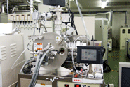
FIB-SEM System;
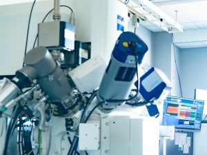
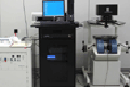
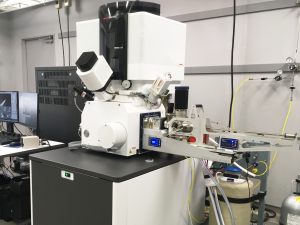 ThermoFisher DualBeam Helios5UX
FIB(Focused Ion Beam) and SEM(Scanning Electron Microscope) combined system with cryo-stage. Preparation of TEM/3DAP samples at low temperature(~around 100K) is available in the machine. In addition, it supports automated FIB fabrication and SEM observation by using Python-based API. Also, transferring 3DAP samples between FIB-SEM and 3DAP machine kept at low temperature and without air exposure is possible by using VCTM(Vacuum and Cryo Transfer Module).
 CarlZeiss CrossBeam550laser
FIB(Focused Ion Beam) and SEM(Scanning Electron Microscope) combined system with a femtosecond laser. Large ROI can be milled by the femtosecond laser, then finely polished by the FIB and observed by SEM. It also supports EDS(Energy Dispersive x-ray Spectroscopy). In addition, preparation of TEM and 3DAP samples by standard lift-out method is possible.
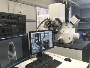 ThermoFisher DualBeam HeliosG4UX
FIB(Focused Ion Beam) and SEM(Scanning Electron Microscope) combined system. In the system, SEM observation, preparation of TEM and 3DAP samples by standard lift-out method are possible. In addition, it supports EDS(Energy Dispersive x-ray Spectroscopy) and EBSD(Electron BackScatter Diffraction) analysis.
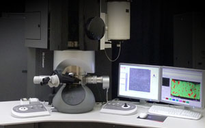
Three-dimensional Atom Probe;
The 3D atom probe method can detect and identify the position of single atoms including light elements, which are difficult to observe with electron microscopes. It is also very effective in analyzing the distribution of elements within a variety of materials or devices.
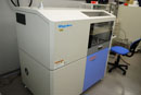
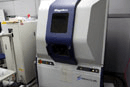
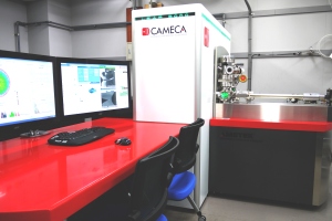 CAMECA LEAP 5000 XS
The LEAP5000XS is a high performance atom probe microscope which provides nano-scale surface, bulk and interfacial materials analysis of simple and complex structures with atom-by-atom identification and accurate spatial positioning.
The system works using the principle of field evaporation, whereby a strong electric field applied to the specimen is sufficient to cause removal of atoms by ionization. Atom removal is triggered either via a voltage or laser pulse applied to the sample. (from the CAMECA's website.)
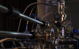 Laser Assisted Wide Angle 3D Atom Probe
Three-dimensional Atom Probe assisted with femtosecond laser pulse. It can analyze wide variety of materials including metals, semiconductors and their devices, ceramics. With shorter flight distance(~12cm), a large angle of view can be achived.
In addition, the development of the microfabrication method using FIB technique makes site specific atomprobe specimen preparation possible, such as grain boundaries, specific region of devices.
Physical and Magnetic Measurement Equipments;
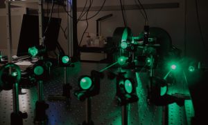
TRMOKE; Time-Resolved Magnet-Optical Kerr Effect Microscope
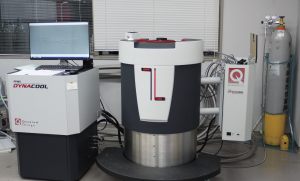
PPMS DynaCool
Lake Shore
VSM 7410
Kerr Microscope
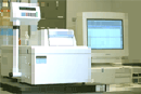
XRF(X-ray Fluorescence) Machine
Rigaku ZSX Primus Ⅱ
Point Contact Andreev Reflection Meausurement System
Vibrating Sample Magnetometer(VSM)
High Sensitive VSM
Differential Thermal Analysis
SQUID-VSM
High-field Micro-Kerr Effect Measuring Equipment
XRD(X-ray diffraction) Machine
Rigaku SmartLab
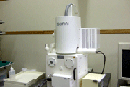
Scanning Electron Microscope
Physical Property Measurement System
Current In Plane Tunnelling
Small ElectroMagnet
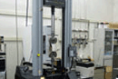
Instron Tensile Test Machine
Alloy & Powder Processing Equipments;
Arc Saction Casting Machine
Arc Melting Furnace
Single Roll Melt Spinner
Vacuum Induction Furnace
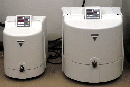
Planetary Ball Mill
Vacuum Glove Box
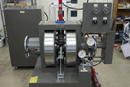
Hydraulic Press Equipment in a Magnetic Field Forming
Infrared Furnace
Magnetic Furnace
Melt Spinning equipment
Hot Press Machine
HDDR process equipment