Orientation-controlled crystalline thin film of perovskite oxide successfully grown on a glass substrate
Use of two-dimensional nanosheets enables high-quality thin film orientation control that requires no single crystal substrate
A research group comprised of Dr. Takayoshi Sasaki, NIMS Fellow, Dr. Tatsuo Shibata, post doctorate researcher, and other collaborators at the International Center for Materials Nanoarchitectonics (MANA; Director: Masakazu Aono) of the National Institute for Materials Science (NIMS; President: Sukekatsu Ushioda) has successfully developed a novel technology to enable oriented growth1) of high quality perovskite oxide thin films, which are important functional materials, in selected preferred orientation on any type of substrate such as a glass substrate.
Many of the advanced electronic and optoelectronic devices around us have incorporated components using crystalline thin films made of various functional materials that play an important part in the devices achieving their functions. Perovskite oxides,2) as typified by barium titanate, represent one such class of functional materials that provides useful characteristics, such as ferroelectricity and piezoelectricity, and they are widely applied to MEMS, sensors and memory. These characteristics depend strongly on such factors as crystal orientation, crystallinity and degree of orientation. Therefore, control of the growth of the thin films poses a decisive challenge. A common choice for growing high-quality, well-oriented crystalline thin films is epitaxial growth4) that uses single crystal substrates3) with a similar crystal structure to that of the target crystal. However, the high cost and size limitations associated with the method prevent wider application. The development of a technology that will enable well-oriented high-quality crystal growth on a cheap and conventional substrate, such as glass and plastics, has been eagerly awaited.
The research group made use of a library of inorganic nanosheets,6) which are graphene-like5) substances obtained by exfoliating a layered compound into single layers. From the library, the group selected three types of oxide nanosheets that were compatible with the structure of the desired orientation, and assembled them on the surface of a glass or other substrate using a solution process, eliminating overlaps and gaps as far as possible, to form an ultra-thin underlayer (seed layer) with a thickness around 1 nanometer. A crystalline thin layer of perovskite-type oxide was deposited on the underlayer by a vapor-phase process. As a result, the group succeeded in growing thin films while controlling their orientations to the (100), (110) and (111) orientations, which are the main orientations used for perovskite crystals, to structurally match the two-dimensional lattice of the respective nanosheets. This technique clearly showed an additional advantage of enabling crystal growth with a higher degree of freedom than in conventional techniques, because unlike an ordinary single crystal substrate surface, nanosheets have no dangling bonds. The obtained thin films showed twice or more greater dielectric performance than non-oriented thin films, demonstrating the effectiveness of this technique from the aspect of functional enhancement.
This research result made it possible to grow perovskite oxide thin films, which are important functional materials, while controlling their orientations, by coating the substrate surface with a nanosheet, which can be considered as a “patterned wallpaper with a nano-level thickness.” Since this new technique is cost-effective and highly universal in that it allows the use of conventional substrates such as glass and plastics that could not be used before and that the nanosheet can be coated onto the substrate surface by a room-temperature solution process, it could have substantial ripple effects on and bring technological innovation in applications to MEMS and sensors.
This research was carried out as part of the research project “Development of Nanomaterials/Manufacturing Processes for Next-generation Electronics Using Inorganic Nanosheets” (Project Leader: Takayoshi Sasaki) in the “Establishment of Innovative Manufacturing Technology Based on Nanotechnology” Research Area of the Core Research of Evolutional Science & Technology (CREST) Program of the Japan Science and Technology Agency (JST). This result will soon be published in Journal of Materials Chemistry C (the Royal Society of Chemistry).
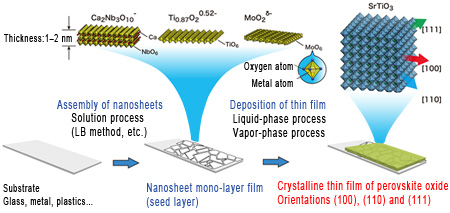
Schematic representation of the technology
Contact information
For more detail about research
Takayoshi Sasaki, MANA Principal Investigator, MANA, NIMS
TEL:+81-29-860-4313
E-mail: sasaki.takayoshi nims.go.jp
TEL:+81-29-860-4313
E-mail: sasaki.takayoshi
nims.go.jpFor general inquiry
Public Relations Office, NIMS
TEL:+81-29-859-2026
FAX:+81-29-859-2017
Email: prnims.go.jp
TEL:+81-29-859-2026
FAX:+81-29-859-2017
Email: pr
nims.go.jp