 Press Release 2012
Success in Development of Metal Oxide Film Transistor with New Compounds
Next-generation Device Enabling Improved Smartphone Battery Life and High Definition in Televisions
A team headed by Dr. Kazuhito Tsukagoshi, a MANA Principal Investigator, and Dr. Toshihide Nabatame, General Manager of the MANA Foundry, of the International Center for Materials Nanoarchitectonics (MANA; Director-General: Masakazu Aono), National Institute for Materials Science (President: Sukekatsu Ushioda), in joint work with Dr. Keiichi Yanagisawa, a technical staff member of the RIKEN Nanoscience Joint Laboratory, succeeded in developing a metal oxide film transistor using a material with an unique atomic composition. Metal oxide film transistors are an object of research and technical development as next-generation materials for amorphous silicon transistors, which are used to switch picture elements (pixels) in the flat panels of existing televisions, computers, smartphones, and similar products. In current displays using amorphous silicon transistors, power consumption is increasing rapidly due to new high resolution and touch panel features.
In recent years, it has been found that IGZO film transistors, which are produced from a mixed target obtained by oxidizing indium, gallium, and zinc, operate with high electron field effect mobility. Although process development is underway aiming at development to practical applications, control of oxygen and moisture is extremely difficult with this material. In this research, an IWO (indium-tungsten oxide) thin film that operates as a thin film transistor was developed by adding an extremely small amount of tungsten oxide to indium oxide. The developed material does not contain gallium or zinc, which are elements that are difficult to control in an amorphous state. Because a homogeneous amorphous film can be produced simply by sputter film-forming at low energy, without heating the substrate or similar operations, thin films are easily formed with this new material, and operation as a transistor with high characteristics is possible, even using a structure without a protective film with an unprecedented thin film thickness of 10nm. In addition to avoiding use of expensive gallium, the thin structure is also effective in reducing material costs because the total amount of raw materials used in the thin film can be reduced, and also enables high production efficiency.
These results were obtained through research with the cooperation of the Materials Division of Sumitomo Metal Mining Co., Ltd.
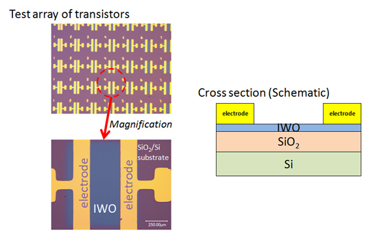
Fig. 1: Optical microscope image and schematic diagram of a prototype device. A thin film was formed from an IWO target by DC sputtering on a SiO2/Si substrate using a room temperature substrate. After forming the electrodes, thermal annealing was performed at 100°C. Device characteristics were measured using the electrodes on the substrate as the source/drain electrodes and the substrate as the gate electrode.
Further information
Affiliation
Kazuhito Tsukagoshi1, Toshihide Nabatame1, Keiichi Yanagisawa2
- International Center for Materials Nanoarchitectonics (WPI-MANA), National Institute for Materials Science (NIMS)
- Nanoscience Joint Laboratory, RIKEN Advanced Science Institute, RIKEN Wako Institute
Contact information
For more detail about research
International Center for Materials Nanoarchitectonics (WPI-MANA),
National Institute for Materials Science (NIMS)
Kazuhito Tsukagoshi, Principal Investigator
mail: <TSUKAGOSHI.Kazuhito nims.go.jp>
TEL:+81-29-860-4894
National Institute for Materials Science (NIMS)
Kazuhito Tsukagoshi, Principal Investigator
mail: <TSUKAGOSHI.Kazuhito
nims.go.jp>TEL:+81-29-860-4894
For general inquiry
Public Relations Office, NIMS
Email: prnims.go.jp
TEL:+81-29-859-2026 FAX:+81-29-859-2017
Public Relations Office, General Affairs Division, RIKEN Headquarter
Email: press-mlaist.go.jp
TEL:+81-29-862-6216 FAX:+81-29-862-6212
Email: pr
nims.go.jpTEL:+81-29-859-2026 FAX:+81-29-859-2017
Public Relations Office, General Affairs Division, RIKEN Headquarter
Email: press-ml
aist.go.jpTEL:+81-29-862-6216 FAX:+81-29-862-6212