 Press Release 2011
Plasmons in nanoscale and atomic-scale systems
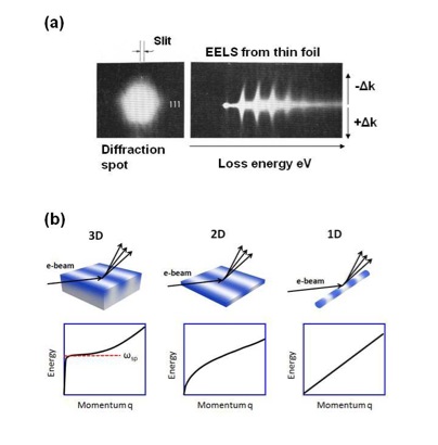
Figure 1 (a) The first observation of a plasmon dispersion curve by using EELS (by H. Watanabe, 1955). ∆k is the momentum of the electron (equal to the momentum q of the excited plasmon) . (b) Schematic diagrams of the reflection EELS measurement of metals with different dimensionalities and their plasmonic bands. ωsp denotes the energy of the surface plasma frequency for the surface of a three-dimensional crystal.
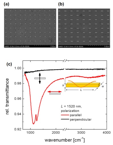
igure 2 (a,b) SEM images of the fabricated nanorod arrays. (c) Relative transmittance spectra of nanorods array at two different polarizations of the incident light: parallel (red curve) and perpendicular (black curve) to the long axis of the nanorods. The rod length is 1520 nm and the width and height of the nanorods are 100 nm. At 1230 cm-1, enhanced sharp signal form the thin (3 nm) dielectric layer between Si and Au appears due to the hybridization between plasmon polaritons of the Au nanoantenna.
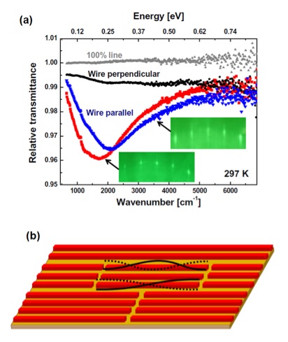
Figure 3 (a) Optical transmittance with electrical field polarized parallel (red squares and blue triangles) and perpendicular (black circles) to the atomic wires (made of In atoms). (b) Schematic illustration of the finite-length indium atomic wires. The wires are segmented by domain boundaries. Dotted and solid curves schematically illustrate the standing-wave 1D plasmons. (In experiment, only the fundamental is observed.)
Further information
Affiliations
- International Center for Materials Nanoarchitectonics (MANA), National Institute for Materials Science (NIMS)
- Kirchhoff Institute for Physics, University of Heidelberg
- Depto de Física de Materiales, Facultad de Ciencias Quimicas, Universidad del Pais Vasco
- Donostia International Physics Center (DIPC)
- IKERBASQUE, Basque Foundation for Science