Observation of Topological Valley Currents
—Observation Using a Graphene Superlattice Device with High Carrier Mobility May Advance the Development of Quantum Electronics—
National Institute for Materials Science (NIMS)
Gunma University
NIMS and Gunma University jointly fabricated a graphene superlattice device with high carrier mobility and succeeded in observing the topological valley current generated in the device. This achievement may facilitate the development of new quantum electronic devices, such as topological superconducting quantum information devices and optical quantum interference devices, which exploit the “valley degrees of freedom”—quantum internal degrees of freedom (i.e., hidden degrees of freedom) of electrons within solid crystals.
Abstract
- NIMS and Gunma University jointly fabricated a graphene superlattice device with high carrier mobility and succeeded in observing topological valley current generated in the device. This achievement may facilitate the development of new quantum electronic devices, such as topological superconducting quantum information devices and optical quantum interference devices, which exploit the “valley degrees of freedom”—quantum internal degrees of freedom (i.e., hidden degrees of freedom) of electrons within solid crystals.
- Electronics in which valley current is used to transmit information are often called “valleytronics.” This technology has been considered a candidate for use in the development of energy-efficient Internet of Things (IoT) devices. Electrons—subatomic particles fundamental to electronics—possess multiple quantum degrees of freedom, including charge degrees of freedom and spin degrees of freedom. Electrons within solid crystals also have another type of quantum degree of freedom called the valley degrees of freedom. The existence of valley degrees of freedom in silicon—a mainstream electronic material today—and in other semiconductor materials has been known for many years. However, the concept of actively utilizing the valley degrees of freedom in devices had not been seriously considered until recently because of difficulty in controlling them.
- Graphene is a monolayer graphite sheet consisting of carbon atoms arranged in a honeycomb pattern. Hexagonal boron nitride also has honeycomb-like atomic arrangement. The fabrication of a superlattice device consisting of graphene and hexagonal boron nitride layers had been thought feasible. Electrons in such a device were predicted to have the valley degrees of freedom, enabling them to simultaneously generate both charge current and the so-called valley current, independently of one another. To test this hypothesis, this research team fabricated a high-quality graphene superlattice device and succeeded in detecting the substantial electrical signals indicative of valley current. In addition, the team demonstrated that the localized electric current detected on the edge of the device may actually be quantum valley current.
- In future studies, the research team plans to apply quantum valley current basic research to the development of new quantum electronic devices, such as optical quantum interference devices, whose valley degrees of freedom can be externally controlled, and topological superconducting quantum information devices.
- This study was carried out by a research team consisting of Katsuyoshi Komatsu (Postdoctoral Researcher, International Center for Materials Nanoarchitectonics [MANA], NIMS; currently affiliated with Toshiba Memory Corporation), Satoshi Moriyama (Senior Researcher, MANA, NIMS) and Yoshifumi Morita (Associate Professor, Graduate School of Science and Technology, Gunma University).
This research will be published in the American scientific journal, Science Advances, at 2:00 pm on May 18, 2018, local time (3:00 am on May 19, Japan Time).
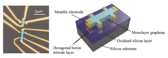
Figure 2 to be used in the press release. Superlattice device composed of graphene and hexagonal boron nitride