Development of Algorithm for Accurate Calculation of Average Distance Travelled by Low-Speed Electrons without Energy Loss that Are Sensitive to Surface Structure
High accuracy achieved in the measurement and analysis of nanosurface materials
2014.08.06
(2014.09.01 Update)
National Institute for Materials Science
The research team consisting of postdoctoral researcher Da Bo, former postdoctoral researcher Hiroshi Shinotsuka, group leader Hideki Yoshikawa and special researcher Shigeo Tanuma, Surface Chemical Analysis Group, Nano Characterization Unit, NIMS; and professor Ding Zejun, University of Science and Technology of China, has developed a theoretical algorithm to accurately calculate the average distance traveled by low-energy/low-speed electrons without energy loss that are sensitive to the surface structures of materials through which they travel while retaining their energy information. The results of this research have been published in Physical Review Letters Vol.113 (2014) 063201. DOI: 10.1103/PhysRevLett.113.063201
Abstract
- The research team consisting of postdoctoral researcher Da Bo, former postdoctoral researcher Hiroshi Shinotsuka, group leader Hideki Yoshikawa and special researcher Shigeo Tanuma, Surface Chemical Analysis Group, Nano Characterization Unit, NIMS (Sukekatsu Ushioda, president); and professor Ding Zejun, University of Science and Technology of China, has developed a theoretical algorithm to accurately calculate the average distance traveled by low-energy/low-speed electrons without any energy loss that are sensitive to the surface structures of materials through which they travel while retaining their energy information. This information on the average traveling distance is vital in terms of measuring the amount of electrons released from materials and gaining information about the depth at which surface analysis is conducted.
- The nanometer-scale surface layers and interface layers influence the properties of various materials such as catalysts, batteries, semiconductors, sensors and anticorrosion materials. It is imperative to identify the amount of elements present and chemical bonding state in these layers in terms of improving the performance of functional materials and developing new materials. And to achieve this, it is essential to accurately analyze and measure electrons (bonding electrons) that indicate the state of elements present in the surface and interface layers. This procedure involves measurement of bonding electron energy extracted from materials due to external stimuli applied to them in such forms as X-rays and electrons, and of the intensity distribution of that energy. During this process, it is critical to identify the depth from the surface at which these measurements were taken. The range of the measurement depth can be determined by measuring a physical quantity called the inelastic mean free path (IMFP), which defines how far an electron can travel in a material while retaining its original energy level in a statistical sense. Experimental and theoretical attempts to quantify IMFP have been pursued globally since the 1970s. However, since it is difficult to take measurements on low-speed electrons that are sensitive to the surface structure (especially at 200eV or below), this quantification had been an issue for a long time.
- In theory, accurate calculation of IMFP in a material is feasible provided that the energy loss function of that material is fully known. The energy loss function represents the level of interaction between the material and electromagnetic waves, and is expressed in terms of the change in the amount of energy lost from electrons and the change in momentum due to corresponding scattering events occurring in the material. The conventional model function (so-called optical energy loss function) only enabled calculating a partial energy loss function under limited conditions assuming zero-momentum, however, lacking of the accompanied changing in momentum as electrons lose energy. As such, this is an incomplete energy loss function in view of obtaining IMFP. The conventional function was particularly problematic when that or similar functions were applied to low-speed electrons that are sensitive to the surface structure. To overcome this problem, we described the optical energy loss function in terms of a composite function resulting from combining many functions, and also used a new model function that accurately expresses the change in momentum. With this method, we succeeded in determining a nearly complete energy loss function. This calculation method enabled us to more accurately perform theoretical prediction of IMFP compared to the experimental value, which was obtained by applying spectrometry (extended X‐ray absorption fine structure spectrometry) to low-speed electrons of Copper and molybdenum at the high-brilliant synchrotron radiation facility, and to explain the relationship between energy measurement and the types of materials. Through this endeavor, we found a hint to solve this long-lasting problem.
- Based on this research, more accurate quantification of elements and analysis of chemical bonding states have become feasible in the several atom thick surface layer of materials using electrons. The results of this study have been published in Physical Review Letters Vol.113 (2014) 063201. DOI: 10.1103/PhysRevLett.113.063201.
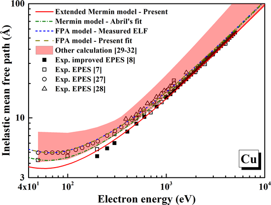
Fig. Inelastic mean free path (IMFP) of copper in relation to electron energy. Theoretical prediction using conventional algorithm (red band), theoretical prediction using newly developed algorithm (red solid line), and experimental data with improved accuracy (■).