On-Demand-Type Device with Switchable Functions Responding to the User’s Needs
Realizes Diverse Functions of Diode, Switch, Capacitor, Brain-Type Memory Device, Etc. in One Device
2012.11.15
(2013.01.07 Update)
National Institute for Materials Science
The NIMS International Center for Materials Nanoarchitectonics (MANA), in joint research with the University of California at Los Angeles (UCLA), succeeded in developing an on-demand-type device which possesses a diverse range of functions, including those of a diode, switch, capacitor, brain-type memory device, in a single device, and realizes the new concept of enabling switching of those functions in response to the user’s needs.
Abstract
- A research group headed by Dr. Rui Yang, a Post-doctoral Researcher at the International Center for Materials Nanoarchitectonics (MANA), National Institute for Materials Science (President: Sukekatsu Ushioda), Dr. Kazuya Terabe, Group Leader of the Nanoionic Device Group, MANA, and Dr. Masakazu Aono, Director-General of MANA, in joint research with Prof. J. Gimzewski of the University of California at Los Angeles, succeeded in developing an on-demand-type device which possesses a diverse range of functions, including those of a diode, switch, capacitor, brain-type memory device, etc. in a single device, and realizes the new concept of enabling switching of those functions in response to the user’s needs.
- Semiconductor devices, represented by transistors, are used as key components of electrical equipment, and their performance is continuing to improve at a rapid pace. However, there are also darkening signs regarding their future development. To continue to improve the performance of electronic information devices in the future, the development of devices based on new operating principles is also important. In this research, an on-demand-type device based on the new concept of switching functions in response to the user’s needs was developed. In conventional semiconductor devices, it was difficult to switch the functions of a device once the device was constructed and configured in a circuit. By using the on-demand-type device developed in this research, it is possible to reduce the number and size of devices in integrated circuits, and furthermore, develop programmable circuits which make it possible to switch the functions of integrated circuits when necessary.
- This on-demand-type device is fabricated using a stacked structure comprising a mixed conductor, in which oxygen ions and electrons can move in a solid, arranged between a pair of metal electrodes. By using the electrochemical reaction and mobility of oxygen ions in the mixed conductor, which depend on the size and frequency of repetition of input electrical signals, it is possible to change the electrical conductivity at the interface between the mixed conductor and the electrodes. The research group successfully realized diverse functions by utilizing these changes in electrical conductivity properties, and also achieved switching of those functions.
- The developed device not only has the functions of a diode, switch, etc., which can also be found in conventional semiconductor devices, but also displays the functions of short-term memory and long-term memory, which are characteristics of the human brain. Therefore, in addition to simple development of existing integrated circuits, this device is expected to make an important contribution to the development of next-generation artificial intelligence by integration with brain-type circuits.
- This research achievement was published in the on-line bulletin of the American scientific journal “ACS Nano” on October 28, 2012 (US time).
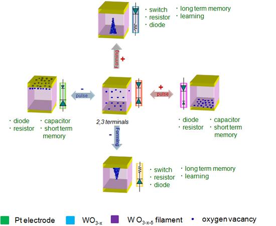
Figure:Diverse functions of the on-demand-type device and method of switching those functions. Electrical conductivity in the vicinity of the interface is expressed by the marks of diode and resistance and their sizes.