Success in Development of Organic Conductive Material Formed at Ultra-High Speed
3-Dimensional Wiring in Next-Generation Multi-Layered Devices Possible at Low Cost
2011.09.21
(2011.10.20 Update)
National Institute for Materials Science
A research group led by Dr. Jin Kawakita, MANA Scientist, and Dr. Toyohiro Chikyo, MANA Principal Investigator, at the International Center for Materials Nanoarchitectonics, National Institute for Materials Science, succeeded in developing a conductive wiring material for electronic applications which enables forming at a growth rate more than 10 times faster than the existing technology.
Abstract
- A research group led by Dr. Jin Kawakita, MANA Scientist, and Dr. Toyohiro Chikyo, MANA Principal Investigator, at the International Center for Materials Nanoarchitectonics (MANA; Director-General: Masakazu Aono), National Institute for Materials Science (President: Sukekatsu Ushioda), succeeded in developing a conductive wiring material for electronic applications which enables forming at a growth rate more than 10 times faster than the existing technology.
- In the electronics field, and particularly in integrated circuits, 3-dimensional layering of devices for high integration has begun. Therefore, how to fabricate multi-layered wiring and wiring in the vertical direction has become an issue. Furthermore, the necessity of multi-layered wiring accompanying high integration has become apparent, including wiring for flexible devices. To meet these needs, new high conductivity wiring materials are demanded. However, forming by the existing wiring fabrication technologies using metal requires many hours, and this is a factor which increases the production cost of electronic component parts.
- In this research, the MANA group succeeded in forming a high conductivity wiring material consisting of a conductive organic polymer and a metal from a solution at a speed more than 10 times faster than the existing technology. This was achieved by simultaneously accelerating the polymerization reaction of the conductive organic polymer and the precipitation reaction of the metal by a light-assisted effect.
- Because this technique enables high speed injection of raw materials in a liquid state and subsequent high speed forming of the conductive material, the filling time for TSV (through-silicon via) in 3-dimensional semiconductors, which is one of the next-generation electronic technologies, is expected to be shortened from the conventional time of several hours to several minutes.
- This result was announced at the Fall Meeting of the Surface Finishing Society of Japan on September 21 and at the Conference on Promotion of Industry-Academic-Government Collaboration on September 22.
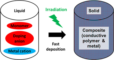
Figure: Forming process for conductive material comprising conductive organic polymer and metal.